. 2019 Dec 13;5(12):eaaw9337.
doi: 10.1126/sciadv.aaw9337. eCollection 2019 Dec.

Spin-charge conversion in NiMnSb Heusler alloy films

Affiliations

Spin-charge conversion in NiMnSb Heusler alloy films

Zhenchao Wen et al. Sci Adv. .

Abstract

Half-metallic Heusler alloys are attracting considerable attention because of their unique half-metallic band structures, which exhibit high spin polarization and yield huge magnetoresistance ratios. Besides serving as ferromagnetic electrodes, Heusler alloys also have the potential to host spin-charge conversion. Here, we report on the spin-charge conversion effect in the prototypical Heusler alloy NiMnSb. An unusual charge signal was observed with a sign change at low temperature, which can be manipulated by film thickness and ordering structure. It is found that the spin-charge conversion has two contributions. First, the interfacial contribution causes a negative voltage signal, which is almost constant versus temperature. The second contribution is temperature dependent because it is dominated by minority states due to thermally excited magnons in the bulk part of the film. This work provides a pathway for the manipulation of spin-charge conversion in ferromagnetic metals by interface-bulk engineering for spintronic devices.


Figures

Fig. 1
Fig. 1. Schematic illustrations for the NiMnSb crystal and electronic band structures.
(A) Crystal structure of NiMnSb in the C1b phase. (B) Half-metallic band structure in NiMnSb. The minority band gap closes because of the interaction between electrons and magnons, i.e., the right-hand side illustration of bulk state. The minority band state exists at the interface/surface (Inter./Sur.). (C) Spin-charge conversion with interface and bulk contributions. Here, JInter.Sur.S and JBulkS represent the spin currents due to interface/surface and bulk, respectively. JTotalC indicates the converted total charge current.
Fig. 2
Fig. 2. Structural properties of NiMnSb films and AMR effect in the films.
(A) Out-of-plane XRD patterns for 20-nm-thick NiMnSb films with two different ordering structures. (B) AMR effect for the two kinds of NiMnSb films measured by an in-plane ϕ scan method at a magnetic field of 2 T at 10 and 300 K, respectively.
Fig. 3
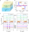
Fig. 3. Voltage measurement with spin pumping.
(A) Schematic illustration of the YIG/NiMnSb sample with experiment setup carried out in the study. (B) Magnetic field dependence of the electronic voltage, V, measured at 10 and 300 K. The directions of external magnetic field, Hex, are also indicated by the inset illustrations. The blue and red solid lines are fitting results for the experimental data by Eq. 1. (C) FMR spectra in YIG (left) and voltage signals in NiMnSb (right) measured in the temperature range from 10 to 300 K. The applied microwave power and frequency here are 25 mW and 5 GHz, respectively.
Fig. 4
Fig. 4. Temperature dependence of VSC with varying microwave power, microwave frequency, and NiMnSb thickness.
(A) VSC as a function of temperature measured at different microwave powers of Pin = 50, 100, and 200 mW, with the microwave frequency of f = 5 GHz. (B) VSC as a function of temperature at different microwave frequencies of f = 5, 6, and 7 GHz with the microwave power of Pin = 25 mW. (C) Temperature dependence of VSC divided by the amplitude of FMR absorption of YIG for NiMnSb films with the thickness of 10, 20, 30, and 50 nm. The VSC measured in a less-ordered NiMnSb film with the thickness of 20 nm is also shown for comparison. The microwave condition is Pin = 25 mW and f = 5 GHz. (D) The dependence of cross temperature, Tcross, for the sign change of VSC on NiMnSb thickness, t. The inset is an enlarged view of (C) in the temperature region below 100 K.
Fig. 5
Fig. 5. Sketch of the voltage due to spin-charge conversion as a function of temperature.
There are two thicknesses, d1 (blue) and d2 (red) (d2 > d1), with the crossing temperatures T1 and T2 (T2 > T1), respectively. The green dashed line is the interfacial contribution V0.
Fig. 6
Fig. 6. Resistivity of NiMnSb films and the voltage due to spin-charge conversion as a function of temperature.
(A) The dependence of the resistivity on temperature for the NiMnSb films with d = 10, 20, 30, and 50 nm. The linear T dependence (~γT) in the high-temperature regime is indicated by a dash-dotted line with the respective value of γ for each thickness. (B) The voltage signal divided by the amplitude of FMR absorption of YIG against the temperature for the various thicknesses of the NiMnSb layer. The symbols represent the experimental data, and the solid line shows their fitted curve with the use of Eq. 9, with V0/PFMR = −0.02 μV/mW, respectively. The shaded areas show the range of fitting curves for −0.03 μV/mW < V0/PFMR < −0.01 μV/mW.

References

    1. Kato Y. K., Myers R. C., Gossard A. C., Awschalom D. D., Observation of the spin Hall effect in semiconductors. Science 306, 1910–1913 (2004). - PubMed
    1. Valenzuela S. O., Tinkham M., Direct electronic measurement of the spin Hall effect. Nature 442, 176–179 (2006). - PubMed
    1. Seki T., Hasegawa Y., Mitani S., Takahashi S., Imamura H., Maekawa S., Nitta J., Takanashi K., Giant spin Hall effect in perpendicularly spin-polarized FePt/Au devices. Nat. Mater. 7, 125–129 (2008). - PubMed
    1. Liu L., Pai C.-F., Li Y., Tseng H. W., Ralph D. C., Buhrman R. A., Spin-torque switching with the giant spin hall effect of tantalum. Science 336, 555–558 (2012). - PubMed
    1. Mellnik A. R., Lee J. S., Richardella A., Grab J. L., Mintun P. J., Fischer M. H., Vaezi A., Manchon A., Kim E.-A., Samarth N., Ralph D. C., Spin-transfer torque generated by a topological insulator. Nature 511, 449–451 (2014). - PubMed

Publication types

LinkOut - more resources