

Junctionless Dual In-Plane-Gate Thin-Film Transistors with AND Logic Function on Paper Substrates
- PMID: 31867536
- PMCID: PMC6921608
- DOI: 10.1021/acsomega.9b03118
Junctionless Dual In-Plane-Gate Thin-Film Transistors with AND Logic Function on Paper Substrates
Abstract
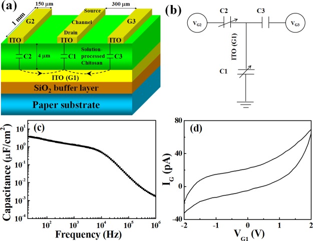
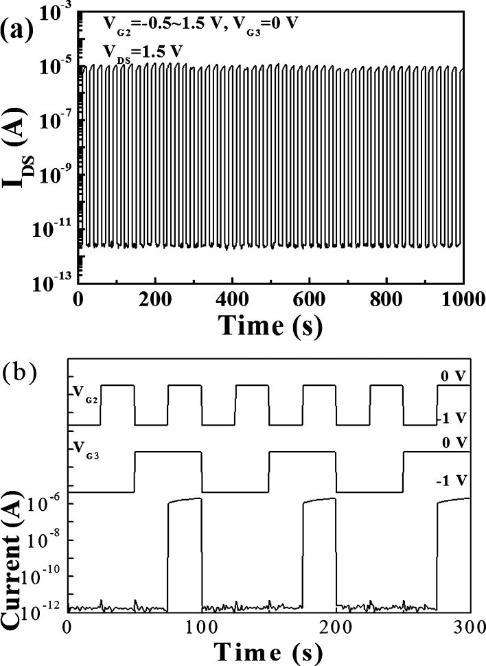
Dual-gate thin-film transistors (DGTFTs) have attracted increasing attention in the past few years because of threshold voltage modulation and device logic functionality. Here, solution-processed chitosan-based proton conductors are used as the gate dielectric. The threshold voltage shift depends on the ratio of the capacitances of the two gate dielectrics. The second interesting application of DGTFTs is logic functionality. This device demonstrates AND logic function controlled by applying either 0 or -1 V to each of the gate electrodes. When both gates were simultaneously applied to be 0 V, the current flows (ON). Otherwise, the current is blocked (OFF). In order to provide a comprehensive overview of these paper devices, the planarization of paper surface and switching stability of such DGTFTs are all discussed.
Copyright © 2019 American Chemical Society.
Conflict of interest statement
The authors declare no competing financial interest.
Figures
Similar articles
-
Dual-gate thin-film transistors, integrated circuits and sensors.Adv Mater. 2011 Aug 2;23(29):3231-42. doi: 10.1002/adma.201101493. Epub 2011 Jun 14. Adv Mater. 2011. PMID: 21671446 Review.
-
Dual Gate Black Phosphorus Field Effect Transistors on Glass for NOR Logic and Organic Light Emitting Diode Switching.Nano Lett. 2015 Sep 9;15(9):5778-83. doi: 10.1021/acs.nanolett.5b01746. Epub 2015 Aug 17. Nano Lett. 2015. PMID: 26274095
-
Low-voltage SnO₂ nanowire transistors gated by solution-processed chitosan-based proton conductors.Nanoscale. 2012 Aug 7;4(15):4481-4. doi: 10.1039/c2nr30969f. Epub 2012 Jul 3. Nanoscale. 2012. PMID: 22760731
-
Self-assembled dual in-plane gate thin-film transistors gated by nanogranular SiO2 proton conductors for logic applications.Nanoscale. 2013 Mar 7;5(5):1980-5. doi: 10.1039/c3nr33734k. Epub 2013 Jan 30. Nanoscale. 2013. PMID: 23364424
-
Split-Gate: Harnessing Gate Modulation Power in Thin-Film Electronics.Micromachines (Basel). 2024 Jan 22;15(1):164. doi: 10.3390/mi15010164. Micromachines (Basel). 2024. PMID: 38276863 Free PMC article. Review.
Cited by
-
Recent Advances in Paper-Based Electronics: Emphasis on Field-Effect Transistors and Sensors.Biosensors (Basel). 2025 May 19;15(5):324. doi: 10.3390/bios15050324. Biosensors (Basel). 2025. PMID: 40422063 Free PMC article. Review.
-
Dual-gate low-voltage transparent electric-double-layer thin-film transistors with a top gate for threshold voltage modulation.RSC Adv. 2020 Mar 3;10(14):8093-8096. doi: 10.1039/c9ra10619g. eCollection 2020 Feb 24. RSC Adv. 2020. PMID: 35497837 Free PMC article.
-
Transparent Structures for ZnO Thin Film Paper Transistors Fabricated by Pulsed Electron Beam Deposition.Micromachines (Basel). 2024 Feb 12;15(2):265. doi: 10.3390/mi15020265. Micromachines (Basel). 2024. PMID: 38398993 Free PMC article.
References
-
- Luo F. C.; Chen I.; Genovese F. C. A thin-film transistor for flat planel displays. IEEE Trans. Electron Devices 1981, 28, 740–743. 10.1109/t-ed.1981.20422. - DOI
-
- Zan H.-W.; Chen W.-T.; Yeh C.-C.; Hsueh H.-W.; Tsai C.-C.; Meng H.-F. Dual gate indium-gallium-zinc-oxide thin film transistor with an unisolated floating metal gate for threshold voltage modulation and mobility enhancement. Appl. Phys. Lett. 2011, 98, 153506.10.1063/1.3578403. - DOI
LinkOut - more resources
Full Text Sources
Other Literature Sources
Miscellaneous