. 2019 Dec 18;6(12):3132-3141.
doi: 10.1021/acsphotonics.9b01196. Epub 2019 Oct 23.

Grayscale-to-Color: Scalable Fabrication of Custom Multispectral Filter Arrays

Affiliations

Grayscale-to-Color: Scalable Fabrication of Custom Multispectral Filter Arrays

Calum Williams et al. ACS Photonics. .

Abstract

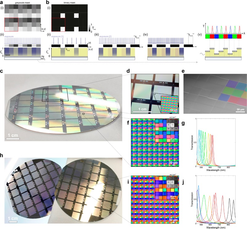
Snapshot multispectral image (MSI) sensors have been proposed as a key enabler for a plethora of multispectral imaging applications, from diagnostic medical imaging to remote sensing. With each application requiring a different set, and number, of spectral bands, the absence of a scalable, cost-effective manufacturing solution for custom multispectral filter arrays (MSFAs) has prevented widespread MSI adoption. Despite recent nanophotonic-based efforts, such as plasmonic or high-index metasurface arrays, large-area MSFA manufacturing still consists of many-layer dielectric (Fabry-Perot) stacks, requiring separate complex lithography steps for each spectral band and multiple material compositions for each. It is an expensive, cumbersome, and inflexible undertaking, but yields optimal optical performance. Here, we demonstrate a manufacturing process that enables cost-effective wafer-level fabrication of custom MSFAs in a single lithographic step, maintaining high efficiencies (∼75%) and narrow line widths (∼25 nm) across the visible to near-infrared. By merging grayscale (analog) lithography with metal-insulator-metal (MIM) Fabry-Perot cavities, whereby exposure dose controls cavity thickness, we demonstrate simplified fabrication of MSFAs up to N-wavelength bands. The concept is first proven using low-volume electron beam lithography, followed by the demonstration of large-volume UV mask-based photolithography with MSFAs produced at the wafer level. Our framework provides an attractive alternative to conventional MSFA manufacture and metasurface-based spectral filters by reducing both fabrication complexity and cost of these intricate optical devices, while increasing customizability.


Conflict of interest statement

The authors declare no competing financial interest.

Figures

Figure 1
Figure 1
Multispectral filter arrays (MSFAs) using grayscale lithography with metal–insulator–metal (MIM) geometry. (a) Schematic: (i) using a customized MSFA atop a monochrome image sensor for multispectral imaging. (ii) 3D MIM structure of MSFA with inset detailing layers. The wavelength transmitted to each pixel below the MIM structures is controlled with the single-step lithographic fabrication process. (b) MSFA fabrication process: (i) a spatially varying grayscale exposure dose results in a spatially varying wavelength transmission profile. (ii) Calculated grayscale exposure dose profile corresponding to remaining resist thickness profiles (“resist sensitivity” curve). An ultrathin noble metal (Ag) layer on glass (SiO2) acts both to dissipate accumulated charge and as the bottom mirror of the filter. (iii) A spatially variant dose modulated exposure leaves a 3D resist profile postdevelopment. (iv) Post-metal-deposition: with a top metal (mirror) layer, the spatially varying 3D resist profile acts to filter the light according to the eigenmode solution of the stack. (v) Final spectral transmittance profiles of MIM structures.
Figure 2
Figure 2
Grayscale exposure dose to color: experimental verification. (a) Finite-difference time-domain (FDTD) simulations of the optical transmission from a continuous Ag-based MIM cavity as a function of varying insulator thickness, with geometry: SiO2(bulk)–Ag(26 nm)–resist (n = 1.653)–Ag(26 nm)–MgF2(12 nm). (b) Experimental demonstration of grayscale-to-dose pattern with the same layers as in (a): (i) Transmission spectra from dose-modulated 5 μm × 5 μm squares (optical micrograph shown in inset), which results in increasing thickness and hence varying peak wavelengths; (ii) measured curve, using an AFM, linking dose and thickness (standard deviation error bars in blue, with overlaid polynomial-fitted red line). Only the first-order resonance is present at low doses, but for higher doses (>50 μC cm–2), the second-order mode is also excited. (c) Dose-modulated 5 μm × 5 μm pixel array with 10 μm spacing: (i) dose-modulated pattern, (ii) optical micrograph, and (iii) corresponding AFM data. (d) Same as (c) but with zero dead space.
Figure 3
Figure 3
Demonstration of the versatility of grayscale MSFAs through patterned design variety. (a) Optical micrograph (with magnified inset) of the University of Cambridge logo text composed of 10 μm pixels with a randomized exposure dose profile, hence random colors in transmission. (b) RGB+NIR MSFA (bands labeled in inset) with (i) optical micrograph in transmission and (ii) respective transmission spectra of the wavelength bands. (c) Photograph of three identically processed chips with a range of patterned designs on each chip with varying complexity. Each chip is processed in a single lithographic step in G-EBL. (d) Spectrally “ordered” 4 × 3 mosaic: (i) optical micrograph; (ii) transmission spectra. (e) 25 μm linearly variable filter pixel design: (i) optical micrograph; (ii) AFM micrograph of the unit cell showing the in-plane height variation. (f) Optical micrograph (with magnified inset) of an array of RGB pixels with exponentially (2n) decreasing pixel width, starting from 10 μm. (g) 25 μm discrete spiral phase pixel design: (i) optical micrograph; (ii) AFM micrograph. Transmission spectra represent averages of five different acquisitions, taken at random positions across the array.
Figure 4
Figure 4
Multispectral imaging through a Bayer filter design and 9-band (3 × 3) MSFA. Bayer filter: (a) Optical micrograph of the mosaic with respective transmission spectra (b) of the 3 bands (RGB). (c) Imaging: Physical representation of the MSFA in front of the image sensor: experimental AFM micrograph, optical micrograph, and image sensor schematic, where d is the distance of the MSFA from the sensor plane (∼1 mm). The experimental imaging setup is shown in SI Figure S16. (d) A snapshot of the imaging test scene, including Macbeth ColorChecker chart and Rubik’s cube, captured with a monochrome image sensor through our mosaic (top) and using a conventional smartphone (bottom), for reference. Aside from demosaicing, there is no postprocessing (enhancement) of the color in the image acquired through our mosaic. 3 × 3 MSFA: (e) Optical micrograph of the 3 × 3 mosaic with respective transmission spectra (f) of the 9 bands (labeled) in the MSFA. (g) Multispectral imaging: Schematic representation of the MSFA in front of the image sensor: experimental AFM micrograph, optical micrograph, and image sensor schematic, where d is the distance of the MSFA from the sensor plane (∼1 mm). 2D intensity matrices from the monochrome image sensor (captured through the MSFA) with illumination from a supercontinuum source are shown in SI Section S 3.3 and SI Video S1 at four different center wavelengths: 500, 550, 600, 650 nm; fwhm 10 ± 2 nm. (h) Multispectral test scene comprising a rear-illuminated filter wheel with four different bandpass filters. (Top) “Raw” color image captured using the monochrome image sensor through our MSFA with individual MSFA pixels visible. (Bottom) Reference image of test scene (comprising 4 bandpass filters across the visible spectrum) taken using a conventional smartphone image sensor. (i) Demosaiced color-coded images for four different wavelength bands obtained from the “raw” image in (h) (top), with labels denoting band.
Figure 5
Figure 5
Wafer-scale grayscale-to-color MSFA fabrication. Photolithography-based MSFA fabrication process flow schematic comparing two proposed approaches: a grayscale photomask (a) or binary photomask (b); both result in equivalent MSFAs. (a) (i) 3 × 3 grayscale photomask: 9 levels of optical transmission, one per spectral band. A single flood exposure can be performed imparting a spatially varying dose profile into the photoresist (ii). (b) (i) 3 × 3 binary photomask: A single transparent pixel is repeated in a 3 × 3 array (MSFA unit cell). The mask is translated in-plane for each spectral pixel, with varying exposure levels (ii–iv). Once processed, the spectral response of the final MSFA (v) is identical to that from (a). (c) Photograph of a 3 in. wafer with ∼32 9-band MSFAs (utilizing second-order resonances), with a zoomed-in region captured with a macro lens (d) and tiled SEM micrograph (e) of the same region. (f) Optical micrograph (transmission) of a different region of the wafer, with labeled equivalent exposure pattern (inset) and corresponding transmission spectra (g) for each spectral band. (h) Photograph of two 3 in. MSFA wafers (utilizing first- and second-order resonances), with optical micrograph of one MSFA (i) and its corresponding transmission spectra for each band (j).

References

    1. Kuroda T.Essential Principles of Image Sensors; CRC Press, 2017.
    1. Lu G.; Fei B. Medical Hyperspectral Imaging: A Review. J. Biomed. Opt. 2014, 19 (1), 01090110.1117/1.JBO.19.1.010901. - DOI - PMC - PubMed
    1. Lapray P. J.; Wang X.; Thomas J. B.; Gouton P. Multispectral Filter Arrays: Recent Advances and Practical Implementation. Sensors 2014, 14 (11), 21626–21659. 10.3390/s141121626. - DOI - PMC - PubMed
    1. Bayer B. E.Color Imaging Array. US3971065A, 1975.
    1. Geelen B.; Tack N.; Lambrechts A.. A Compact Snapshot Multispectral Imager with a Monolithically Integrated Per-Pixel Filter Mosaic. Proc. SPIE 2014, 8974, 89740L.10.1117/12.2037607. - DOI