. 2020 Feb 19;142(7):3513-3524.
doi: 10.1021/jacs.9b12424. Epub 2020 Feb 7.

Protective Layers Based on Carbon Paint To Yield High-Quality Large-Area Molecular Junctions with Low Contact Resistance

Affiliations

Protective Layers Based on Carbon Paint To Yield High-Quality Large-Area Molecular Junctions with Low Contact Resistance

Senthil Kumar Karuppannan et al. J Am Chem Soc. .

Abstract

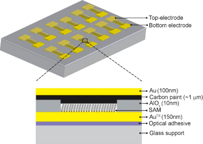
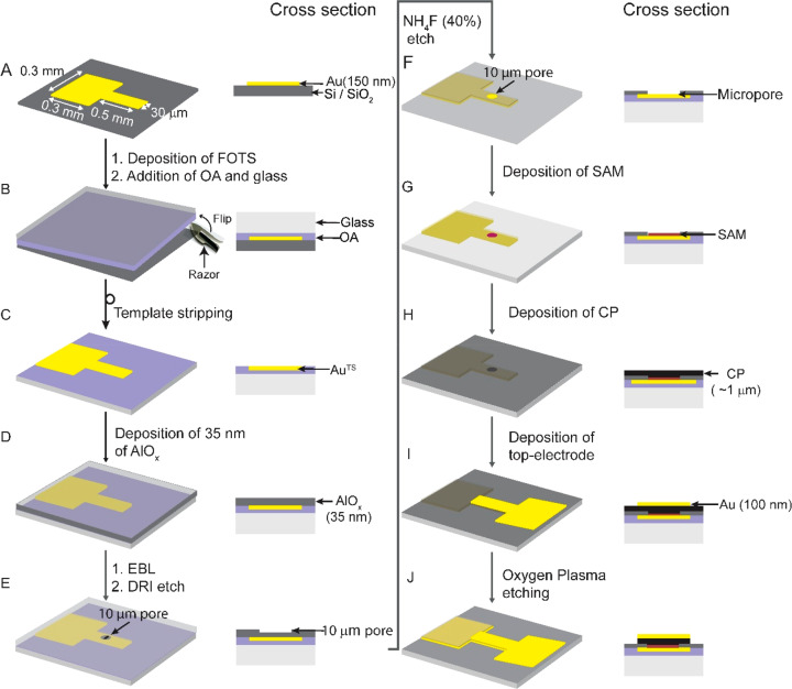
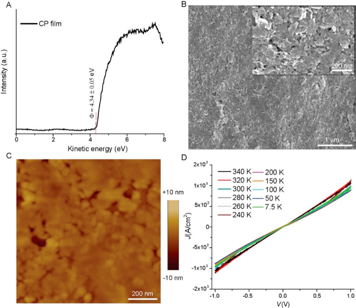
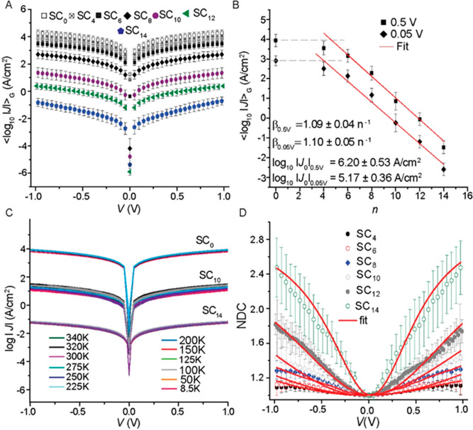
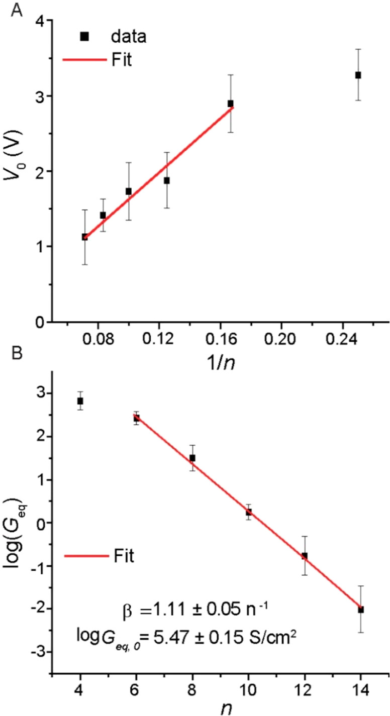
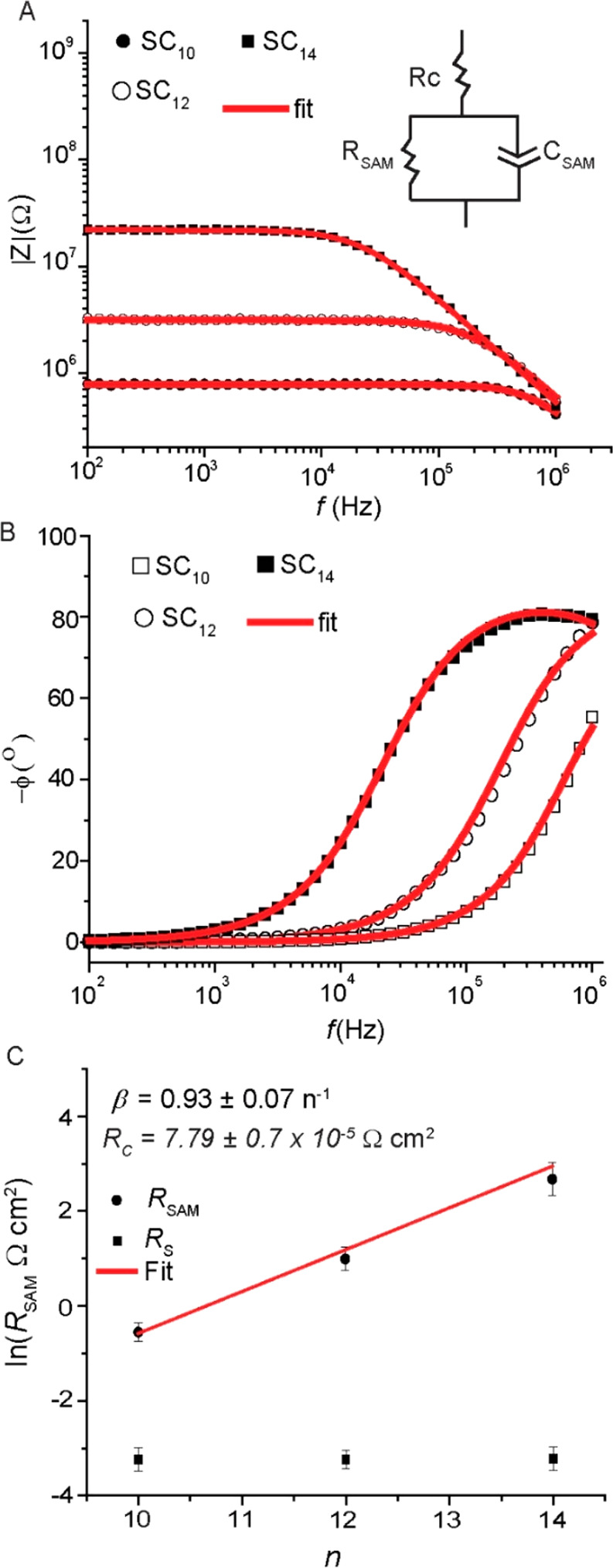
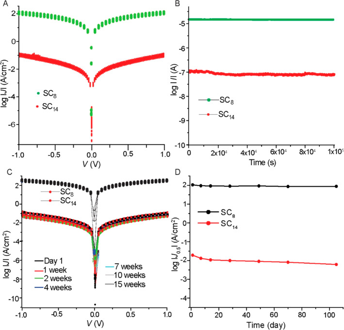
A major obstacle for transforming large-area molecular junctions into a viable technology is the deposition of a top, metallic contact over the self-assembled monolayer (SAM) without chemically damaging the molecules and preventing an interface-limited charge transport. Often a thin conducting layer is softly deposited over the SAM to protect it during the deposition of the metal electrode which requires conditions under which organic molecules are not stable. We report a new protective layer based on carbon paint which is highly conductive and has metallic-like behavior. Junctions made of SAMs of n-alkanethiolates supported by Au were characterized with both dc and ac techniques, revealing that carbon paint protective layers provide a solution to three well-known challenges in molecular junctions: series resistance of the leads, poor interface conductance, and low effective contact area related to the roughness of the interfaces. Transport is constant with coherent tunneling down to 10 K, indicating the carbon paint does not add spurious thermally activated components. The junctions have both high reproducibility and good stability against bias stressing. Finally, normalized differential conductance analysis of the tunneling characteristics of the junctions as a function of molecular length reveals that the scaling voltage changes with molecular length, indicating a significant voltage drop on the molecules rather than on the molecule-electrode interface. There is a clear inverse dependence of the scaling voltage on length, which we deduced has a tunneling barrier height of close to 2 eV. The paper establishes the reliability of carbon paint protective layers and provides a procedure for discriminating genuine molecular effects from interfacial contributions.


Conflict of interest statement

The authors declare no competing financial interest.

Figures

Figure 1
Figure 1
Schematic illustration of the molecular tunnel junction (AuTS–SCn//CP//Au) with carbon paint (CP) as a protective layer: TS indicates template stripped, “–” indicates a covalent interface, and “//” indicates a noncovalent interface.
Figure 2
Figure 2
Fabrication process of the AuTS–SCn//CP//Au junctions based on SAMs on template-stripped Au inside micropores (with a diameter of 10 μm) with a carbon paste (CP) protective layer and Au top contacts. All fabrication steps are explained in the main text.
Figure 3
Figure 3
(A) Ultraviolet photoelectron spectra of the CP film which was obtained by templating the CP film from AuTS–SC12 with Scotch tape. (B) Scanning electron microscopy image of spin-coated CP film. (C) Atomic force microscope image of CP, which was obtained by template stripping the CP film from AuTS–SC12 with Scotch tape. (D) J(V) characteristics of a AuTS//CP//Au junction as a function of temperature.
Figure 4
Figure 4
(A) ⟨log10 |J|⟩G vs V traces of AuTS–SCn//CP//Au junctions. (B) Value of ⟨log10 |J|⟩G (measured at V = +0.5 and +0.05 V) plotted against the number of carbons, n; dashed gray lines indicate the current across the control device without a SAM; red solid lines are fits to eq 2. (C) J(V) characteristics as a function of T for junctions with n = 10 or 14 or without a SAM for T = 8.5–340 K. (D) Normalized differential conductance vs V for junctions with n = 4, 6, 8, 10, 12, and 14. Error bars represent 99% confidence levels, and solid red lines are fit to eq 5.
Figure 5
Figure 5
(A) Plot of transition voltage (V0) vs 1/n (error bars represent the standard deviation from five independent JV traces). (B) Plot of log(Geq) vs n; solid line is a fit to eq 8.
Figure 6
Figure 6
(A) Frequency dependency of |Z| of the junctions at zero bias for micropore device with SAM of SCn with n = 10, 12, or 14. (B) Corresponding phase angle (ϕ) vs frequency plots. (C) Resistance of the SAM (RSAM) and the contact resistance (RC) vs the number of carbons; red line is a fit to eq 9.
Figure 7
Figure 7
Stabilities of the junctions with SAMs SC8, SC14, and SC14. (A) 2000 J(V) curves measured by continuously sweeping the bias between +1.0 and −1.0 V. (B) Retention characteristics at +1.0 V for 1.02 × 10⁵ s while measuring the current at 15 s intervals. (C) J(V) curves of junctions and (D) value of J at 0.5 V measured within 1 day after fabrication and after aging for 15 weeks in ambient conditions (at 24 °C in air, relative humidity of 60%).

References

    1. Vilan A.; Aswal D.; Cahen D. Large-Area, Ensemble Molecular Electronics: Motivation and Challenges. Chem. Rev. 2017, 117, 4248–4286. 10.1021/acs.chemrev.6b00595. - DOI - PubMed
    1. Metzger R. M. Unimolecular Electronics. Chem. Rev. 2015, 115, 5056–5115. 10.1021/cr500459d. - DOI - PubMed
    1. Van Hal P. A.; Smits E. C. P.; Geuns T. C. T.; Akkerman H. B.; De Brito B. C.; Perissinotto S.; Lanzani G.; Kronemeijer A. J.; Geskin V.; Cornil J.; Blom P. W. M.; De Boer B.; De Leeuw D. M. Upscaling, Integration and Electrical Characterization of Molecular Junctions. Nat. Nanotechnol. 2008, 3, 749–754. 10.1038/nnano.2008.305. - DOI - PubMed
    1. Xiang D.; Wang X.; Jia C.; Lee T.; Guo X. Molecular-Scale Electronics: From Concept to Function. Chem. Rev. 2016, 116, 4318–4440. 10.1021/acs.chemrev.5b00680. - DOI - PubMed
    1. Jeong H.; Kim D.; Xiang D.; Lee T. High-Yield Functional Molecular Electronic Devices. ACS Nano 2017, 11, 6511–6548. 10.1021/acsnano.7b02967. - DOI - PubMed