

doi: 10.1088/2050-6120/ab6ed7.
Wide-field time-gated SPAD imager for phasor-based FLIM applications
Affiliations
- PMID: 31968310
- PMCID: PMC8827132
- DOI: 10.1088/2050-6120/ab6ed7
Item in Clipboard
Wide-field time-gated SPAD imager for phasor-based FLIM applications
Methods Appl Fluoresc.
.
Abstract
We describe the performance of a new wide area time-gated single-photon avalanche diode (SPAD) array for phasor-FLIM, exploring the effect of gate length, gate number and signal intensity on the measured lifetime accuracy and precision. We conclude that the detector functions essentially as an ideal shot noise limited sensor and is capable of video rate FLIM measurement. The phasor approach used in this work appears ideally suited to handle the large amount of data generated by this type of very large sensor (512 × 512 pixels), even in the case of small number of gates and limited photon budget.
Figures

Characteristics of the gate used in the FLIM experiment. The response of
every other 4th pixel in the center 472 × 256 array is plotted. The
minimum achievable gate length is 10.8 ns.

(a) Microscopic image of SS2 pixels with microlenses. Scale bar is 200
μm. (b)–(c) Fluorescence intensity image of a
convallaria majalis sample captured with SS2 (b) without and (c) with
microlenses [22]. Mean photon count
without microlenses: 41.4. Mean photon count with microlenses: 109.6. Microlens
concentration factor: 2.65. Experimental parameters: Vex: 6.5 V,
array size: 453 × 210, bit depth: 10, integration time: 3.21 ms,
λemission: 607 nm, pile-up correction:
on. Hot pixels with 1% highest dark count rate in the array were corrected using
an interpolation method based on setting their intensity values to the mean of
the four nearest-neighbor pixels.

Conceptual illustration of the phasor method. (a) A gate with a fixed
width W is scanned across the 50 ns fluorescence decay period. Each gate is
associated with a ‘nanotime’ specifying its start time with
respect to the laser pulse. Each pixel in a gate image contains the number of
photons detected during the gate image exposure time. (b) The phasor of the
decay (P) recorded in a given pixel is calculated as the
weighted average of the gate image intensity multiplied by a cosine or sine term
depending on the gate nanotime (equation
(3)). For a single-exponential decay, P is located
on the universal semicircle, approaching the origin point (0, 0) as lifetime
increases toward infinity. The phase lifetime is calculated using
φ, the angle of the line connecting
P to the origin according to equation (4).

Conceptual illustration of mixture analysis. P is the
phasor of the mixture, τ1
and τ2 are the phasors of
two dyes, and d1 and
d2 are the distances between
the phasors of the dyes and the mixture. The phasor ratio can be found by
calculating the ratio of the phasor distances, then can be converted to volume
fraction using equation
(16).

Gate intensity profiles (coordinates (193,190)) of (a) ATTO 550, (b)
Cy3B, (c) Rhodamine 6G (R6G), and (d) quantum dot (QD585) solutions. Parameters:
laser frequency: 20 MHz, gate width W = 13.1 ns, bit depth: 10, background
correction: off. Blue: no pile-up correction, red: pile-up correction.
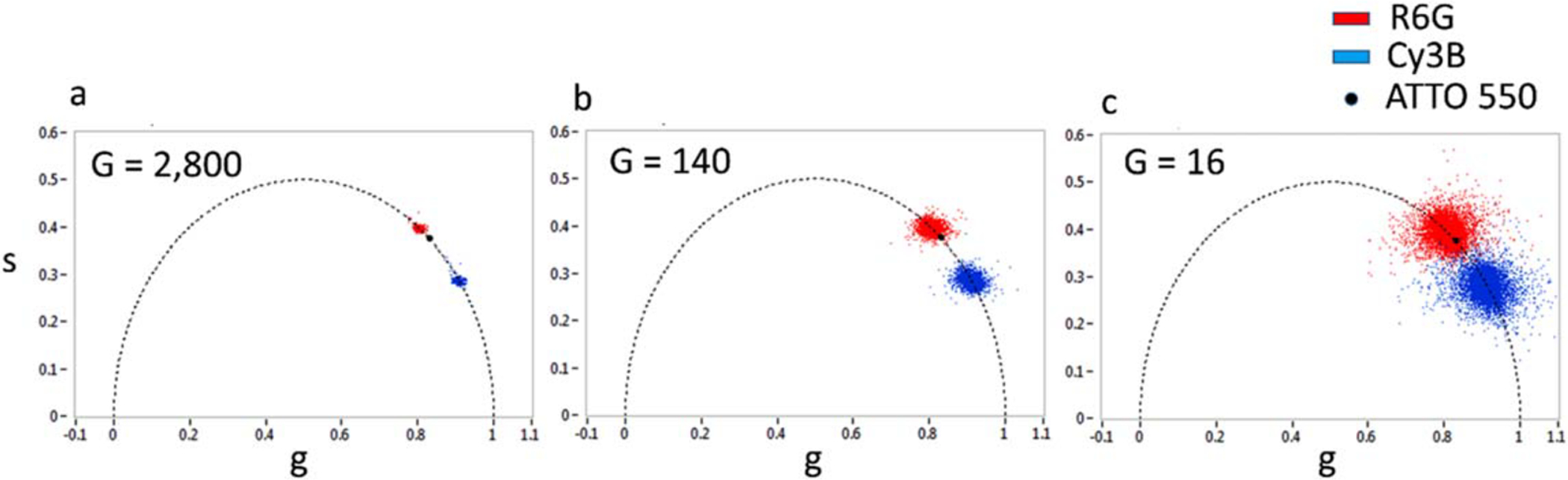
Phasor scatter plots for the R6G (τ = 4.08 ns)
and Cy3B (τ = 2.8 ns) solutions obtained with 2,800 (a),
140 (b) and 16 (c) gate positions and calibrated with the corresponding ATTO 550
dataset (τ = 3.6 ns). The visual separation of the
phasors of the two samples becomes more challenging when fewer gates (and thus
fewer photons) are used. Even with as low as 16 gates, the two samples are
clearly distinguishable. Experiment parameters: laser and phasor frequency: 20
MHz, gate width: 13.1 ns, array size: 472 × 256, binning: 4 × 4,
bit depth: 8 (R6G & Cy3B), 16 (ATTO 550), pile-up correction: on, background
correction: on, percentage of removed pixels: 0% (R6G & Cy3B), 0.5% (ATTO
550).

FLIM performance of SS2 for different effective acquisition frame rates,
determined by the number of gate positions (# Gates = G). The
numbers G used here are 2,800, 1,400, 700, 350, 175, 80, 40, 16
and 8: (a): Phase lifetime ± standard deviation. The dashed lines
indicate the literature values for both lifetimes. (b): standard deviation. The
dashed lines indicate a G−1/2 dependence.
(c): total photon counts per 4 × 4-pixel ROI. The dashed lines indicate a
linear dependence on G. (d): F-value of ATTO
550 and R6G data sets. The dashed lines indicate the Monte Carlo estimation of
the effect of shot noise. Experimental parameters: laser & phasor frequency:
20 MHz, gate width: 13.1 ns, array size: 472 × 256, binning: 4 ×
4, bit depth: 8, pile-up correction: on, background correction: on.

Dependence of the measured phase lifetime on gate width. (a): Average
phase lifetime of the ATTO 550 and R6G samples calibrated with the Cy3B sample
(τ = 2.8 ns) using 140 gates. The points represent
the average of all values in the image, while the error bars correspond to the
measured standard deviation. The plain lines correspond to the average of all
values; the dashed lines indicate the literature values for both dyes. (b), (c):
Dependence of the phase lifetime standard deviation on gate width, for
G = 140 (b) and G = 16 (c) gates. Points:
measured values; plain lines: results of equation (13); dashed lines: MC results. (d):
Dependence of the F-value on gate width. Filled symbols: G =
16, open symbols: G = 140: plain lines: results of equation (14); dashed lines: MC
results. Experimental parameters: laser & phasor frequency: 20 MHz, number
of gate positions: 16 or 140, array size: 476 × 256, binning: 4 ×
4, bit depth: 8, background correction: on, pile-up correction: on.

Dye mixture analysis of Cy3B and R6G with various volume fractions. A
separate Cy3B sample was used as the reference dye for phasor calibration, using
a τ = 2.5 ns (value measured by TCSPC).
μ is the initial dye concentration ratio and
χ is the product of the extinction coefficient ratio
and quantum yield ratio for both dyes [28]. (a) Phasors of the dyes (red) and mixtures (green) on the universal
semicircle. (b) Calculated μχ for each mixture,
and the μχ obtained by fitting method.
Experimental parameters: laser PRF: 20 MHz, phasor frequency: 20 MHz, number of
gate positions: 234, gate length: 22.8 ns, array size: 248 × 160,
binning: 8 × 8, bit depth: 10, pile-up correction: on, background
correction: on, percentage of removed pixels: 1%. Note that because the mixtures
decays are not single-exponential, a constant background subtraction approach
was used based on the background measured in the reference sample.

QD phase lifetime map. (a): Intensity image of a dried QD sample. The
contrast has been adjusted to be able to see most of the field of view. Scale
bar: 25 μm. (b), (c): Color-coded phase lifetime maps.
Two references (green dot: 16.7 ns and red dot: 13.9 ns) were defined in the
phasor plot shown in (d). Pixels were color-coded according to the their phasor
ratio with respect to these two references and using the
‘spectrum’ color scale indicated in b. Pixels with phasors close
to the first reference (green dot: longer lifetimes) were colored blue, while
pixels with phasors close to the second reference (red dot: shorter lifetimes)
were colored red. Pixels with phasors in between were colored with an
intermediate color. Points outside the segment were colored according to the
closest point on the segment. The elongated hexagon represents the boundary of
the region of the phasor plot were this color-coding scheme applies. In b, the
luminance is kept identical for all pixels, irrespective of their actual
intensity allowing to visualize low intensity pixels (and their phase
lifetimes). There is no obvious correlation between lifetime and intensity,
while there appears to be a correlation between concentration and lifetime. In
c, the luminance of each pixel scales with its intensity (shown in a). (d):
Bottom: Phasor plot of the data shown in a. Top: detail of the square region
selected in the bottom phasor plot. The two references (green and red dots) are
visible at both extremities of the phasor cloud.
References
-
- Suhling K, French PMW and Phillips D 2005. Time-resolved fluorescence microscopy Photoch. Photobio. Sci 4 13–22 - PubMed
-
- Borst Jan Willem and Visser Antonie J W G 2010. Fluorescence lifetime imaging microscopy in life sciences Meas. Sci. Technol 21 102002
-
- Joseph Lakowicz 2006. Principles of Fluorescence Spectroscopy 3 (New York: Springer; ) 978-0-387-31278-1 (10.1007/978-0-387-46312-4) - DOI
-
- Hirvonen Liisa M and Suhling Klaus 2017. Wide-field TCSPC: methods and applications Meas. Sci. Technol 28 012003