. 2020 Apr;83(4):044101.
doi: 10.1088/1361-6633/ab72e5. Epub 2020 Feb 4.

Recent advances in infrared imagers: toward thermodynamic and quantum limits of photon sensitivity

Affiliations

Recent advances in infrared imagers: toward thermodynamic and quantum limits of photon sensitivity

Simone Bianconi et al. Rep Prog Phys. 2020 Apr.

Abstract

Infrared detection and imaging are key enabling technologies for a vast number of applications, ranging from communication, to medicine and astronomy, and have recently attracted interest for their potential application in optical interconnects and quantum computing. Nonetheless, infrared detection still constitutes the performance bottleneck for several of these applications, due to a number of unsolved challenges, such as limited quantum efficiency, yield and scalability of the devices, as well as limited sensitivity and low operating temperatures. The current commercially dominating technologies are based on planar semiconducting PIN or avalanche detectors. However, recent developments in semiconductor technology and nano-scale materials have enabled significant technological advancement, demonstrating the potential for groundbreaking achievements in the field. We review the recent progress in the most prominent novel detection technologies, and evaluate their advantages, limitations, and prospects. We further offer a perspective on the main fundamental limits on the detectors sensitivity, and we discuss the technological challenges that need to be addressed for significative advancement of the field. Finally, we present a set of potential system-wide strategies, including nanoscale and low-dimensional detectors, light coupling enhancement strategies, advanced read-out circuitry, neuromorphic and curved image sensors, aimed at improving the overall imagers performance.


Figures

Figure 1
Figure 1
a) Comparison of detectivity (D*) of various commercially available infrared detectors operating at the indicated temperature[2]; b) The absorption spectrum of Earth’s atmosphere [13].
Figure 2
Figure 2
History of the development of infrared detectors and systems, with the four generations of infrared imagers, as proposed by Rogalski et al.[27]. Highlighted in blue are the major novel detector concepts developed over the last three decades. The inset shows the evolution of the number of pixels in MWIR FPAs over time, which follows Moore’s law exponential trend. Adapted from [27].
Figure 3
Figure 3
SWIR imager research output over the last 20 years. a) SWIR detection citation report for the most common and most promising technologies: the citation boost is dominated by low-dimensional materials (b) and III-V and Ge-based detectors, particularly involving Si integration methods (c). Note: 2019 data only include citations from January though October.
Figure 4
Figure 4
Absorption coefficient (a) and normalized detectivity (b) as a function of wavelength for detectors based on different materials. The normalized detectivityD* is calculated from eq. 10, assuming a background temperature of 300 K and a field of view of 30°.
Figure 5
Figure 5
Effect of detector size on the radiance and detectivity. a) Modified blackbody spectra Bbb(v, T, d)for different detector sizes (solid lines). The corresponding correction factors are represented by the dashed lines and refer to the right y-axis. The spectra correspond to radiance emitted by a blackbody at 5000 K. b) and c) Normalized detectivity D* as a function of wavelength for different detector sizes, for Hg0.5Gd0.5Te-based (b) and In0.53Ga0.47As-based (c) detectors. D* was calculated from eq. 10 and 12, assuming a background temperature of 300 K and a field of view of 30°. d) Normalized detectivity D* of an In0.53Ga0.47As-based detector at 1500 nm as a function of background temperature for different detector sizes, calculated from eq. 10 and 12, assuming a field of view of 30°.
Figure 6
Figure 6
Detectivity enhancement enabled by sub-wavelength sized detectors for common detector materials across the infrared and visible range. a) Solid lines represent the detectivity D*, calculated from eq. 10 and 12, assuming a background temperature of 300 K and a field of view of 30°, for a bulk detector (size much greater than wavelength). Dashed lines represent the enhanced detectivities enabled by the modified blackbody spectra Bbb(v, T, d) for subwavelength detector sizes. b) Relative detectivity enhancement (ratio of modified subwavelength detectivity to bulk).
Figure 7
Figure 7
a) Circuit equivalent of e phototransistor detector, as proposed in Rezaei et al. [42]; b) Schematic of a photocurrent pulse in a detector, showing the two different regimes; c) Detector SNR as a function of detector size for three different absorbed photons fluxes; c) Detector sensitivity in number of absorbed photons detected with a certain SNR as a function of detector size. In both c) and d), the solid line represents the solutions for T = 300 K, the dashed lines for T = 77 and the dotted lines for T = 4 K.
Figure 8
Figure 8
Direct and indirect bandgap and corresponding cutoff wavelength of some of the most common semiconductors in IR detection application[28].
Figure 9
Figure 9
Band gap and corresponding cutoff wavelength EG=hcλ of Hg1-xCdxTe near the T -point for varying x-composition of the alloy[28].
Figure 10
Figure 10
a) Band diagram schematic of APD detectors [101]; b) Voltage dependency of the avalanche gain in SAPHIRA APD FPA[45]; c) Electron and hole avalanche multiplication gain as a function of HgCdTe bandgap [28]; d) RAPID [103] 320×255 IR APD array integrated in cryostat
Figure 11
Figure 11
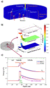
a) Schematic of the geometric design of the EI detector, combining a large-area absorption region with a small-volume hole-trapping multiplication region (nanoinjector)[115]; Cross-sectional 3D (b) and axial (c) band structure showing lateral band bending for charge compression and confinement[116, 119].
Figure 12
Figure 12
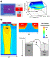
a) Top-view schematic and 3D potential profile in a pump-gate jot [112]. b) Cross sectional potential profiles along lines aa’ and bb’, and band diagram schematic of the two steps of pump action, corresponding to transfer gate (TG) on and off along the charge transfer path[112]: SW indicates the storage well, PB and PW a p-type barrier and well respectively, VB the virtual phase barrier, and FD the floating diffusion. Adapted with permission from ref.[112], OSA.
Figure 13
Figure 13
Schematic diagram of the triple-band superlattice SWIR-MWIR-LWIR photodetector reported by Hoang et al. [110]. The band alignment of the three different superlattices employed are reported on the right (colored squares represent the forbidden bandgaps and the dashed lines the effective bandgaps). (image adapted from [110] https://creativecommons.org/licenses/by/4.0/)
Figure 14
Figure 14
Low-dimensional photodetector architectures based on QD (a) [49], nanowires (b) [123], and 2D material (c) [124]
Figure 15
Figure 15
a) Nano-structured Si cones for MWIR AR application(adapted from [133]); b) Schematic of a cavity-based IR detector architecture for enhanced quantum efficiency, adapted with permission from ref. [134], OSA.
Figure 16
Figure 16
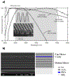
a) Microscope image of the fabrication steps for microlens arrays[137]; b) Scanned electron image and schematic of light concentrators array for HgCdTe FPA[45]; c) Image of a quasi-flat achromatic lens based on space-varying dielectric gradient metastructure, with ~ 2 μm measured spot size from 1200 nm to 1600 nm wavelengths, (image adapted from [141] https://creativecommons.org/licenses/by/4.0/)
Figure 17
Figure 17
a) Schematic of a nanoholes-array photonic crystal slab and modes of field distribution [142]; b) Schematic of plasmonics-enhanced graphene photodetector architecture[143]; c) Schematic of PC-based resonator implementation in an FPA [144]; d) Schematic and FDTD field enhancement simulation for the hybrid metallo-dielectric photonic jet nanoantenna [148]. Panels a, c, d are adapted with permission from refs.[142, 144, 148], OSA.
Figure 18
Figure 18
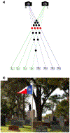
a) Schematic of artificial stereo vision employing two cameras (left, L and right, R), with representation of a typical correspondence problem (the four red dots representing the solution)(image adapted from[163], .https://creativecommons.org/licenses/by/4.0/). b) Example of foveated image with point of fixation on the Stephen F. Austin statue in the background adapted from en.wikipedia.org/wiki/Foveated_imaging#/media/File: Texas_state_cemetery_foveated1.png
Figure 19
Figure 19
a) Schematic of the eye’s aberration-free curved imaging sensor, compared to the aberration from a single thick lens related with a planar imager. b) 8 megapixel CMOS curved imager bonded to a precisely curved mold surface (adapted from [164]).

Similar articles

Cited by

References

    1. Fang Y, Armin A, Meredith P and Huang J, “Accurate characterization of next-generation thin-film photodetectors,” Nature Photonics, vol. 13, pp. 1–4, 2019.
    1. Rogalski A, Infrared detectors, CRC press, 2010.
    1. Herschel W, “Experiments on therefrangibility of the invisible rays of the sun,” Phylosophical Transactions of the Royal Society of London, vol. 90, no. 284, 1800.
    1. Case TW, “The Thalofide cell: a new photoelectric substance,” Physical Review, vol. 15, no. 289, 1920.
    1. Hudson RD and Hudson JW, Infrared detectors, Stroudsburg, PA: Dowden, Hutchinson & Ross, 1975.

LinkOut - more resources