

Printed Electronics as Prepared by Inkjet Printing
- PMID: 32033206
- PMCID: PMC7040650
- DOI: 10.3390/ma13030704
Printed Electronics as Prepared by Inkjet Printing
Abstract
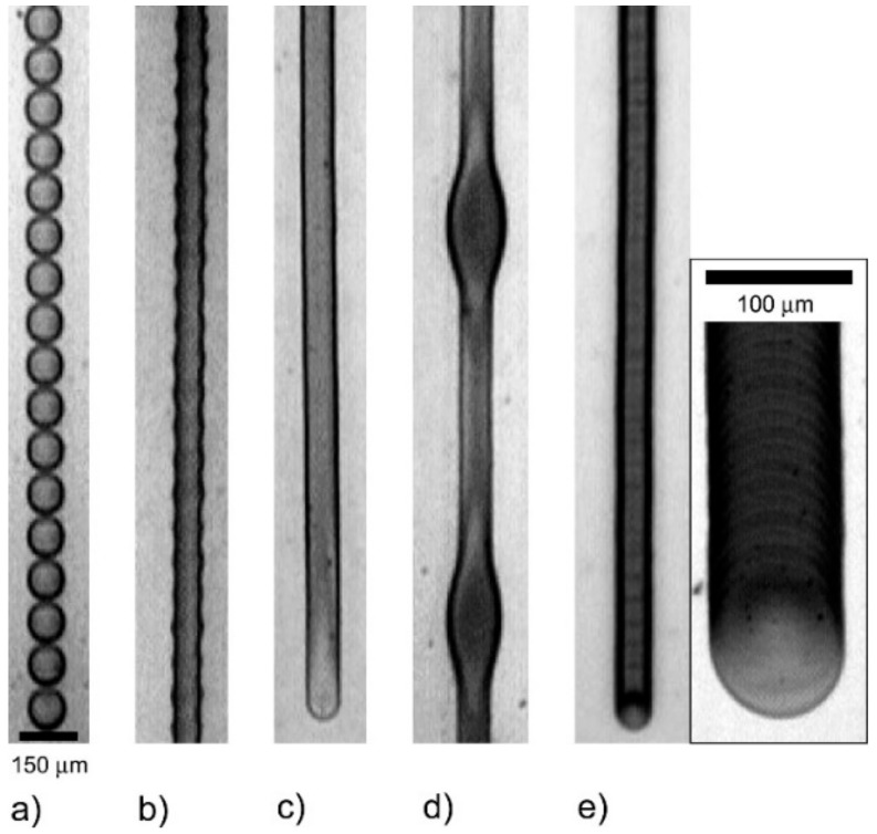
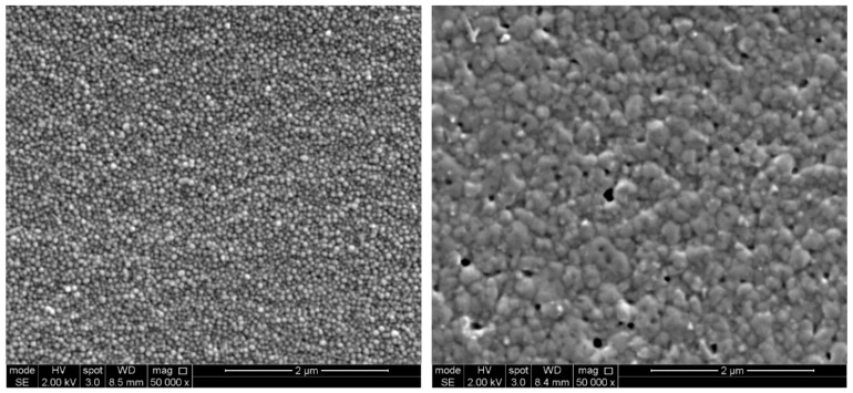
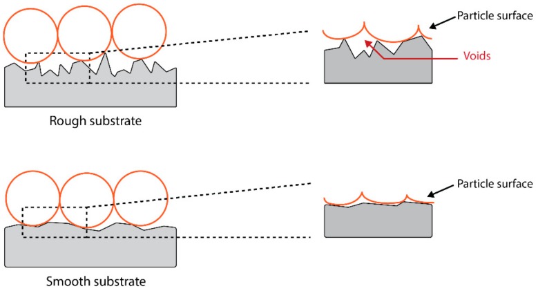
Inkjet printing has been used to produce a range of printed electronic devices, such as solar panels, sensors, and transistors. This article discusses inkjet printing and its employment in the field of printed electronics. First, printing as a field is introduced before focusing on inkjet printing. The materials that can be employed as inks are then introduced, leading to an overview of wetting, which explains the influences that determine print morphology. The article considers how the printing parameters can affect device performance and how one can account for these influences. The article concludes with a discussion on adhesion. The aim is to illustrate that the factors chosen in the fabrication process, such as dot spacing and sintering conditions, will influence the performance of the device.
Keywords: adhesion; droplet behavior; electrical conductivity; ink; inkjet printing; laser sintering; printed electronics.
Conflict of interest statement
The authors declare no conflicts of interest.
Figures
Similar articles
-
Inkjet Printing of Polyacrylic Acid-Coated Silver Nanoparticle Ink onto Paper with Sub-100 Micron Pixel Size.Materials (Basel). 2019 Jul 15;12(14):2277. doi: 10.3390/ma12142277. Materials (Basel). 2019. PMID: 31311191 Free PMC article.
-
All Inkjet-Printed Graphene-Silver Composite Ink on Textiles for Highly Conductive Wearable Electronics Applications.Sci Rep. 2019 May 29;9(1):8035. doi: 10.1038/s41598-019-44420-y. Sci Rep. 2019. PMID: 31142768 Free PMC article.
-
Wetting Behavior of Inkjet-Printed Electronic Inks on Patterned Substrates.Langmuir. 2024 Mar 12;40(10):5162-5173. doi: 10.1021/acs.langmuir.3c03297. Epub 2024 Feb 26. Langmuir. 2024. PMID: 38408752 Free PMC article.
-
A Review on Sustainable Inks for Printed Electronics: Materials for Conductive, Dielectric and Piezoelectric Sustainable Inks.Materials (Basel). 2023 May 24;16(11):3940. doi: 10.3390/ma16113940. Materials (Basel). 2023. PMID: 37297073 Free PMC article. Review.
-
Copper inks for printed electronics: a review.Nanoscale. 2022 Nov 10;14(43):16003-16032. doi: 10.1039/d2nr03990g. Nanoscale. 2022. PMID: 36301077 Review.
Cited by
-
Three-Dimensional Printing of Multifunctional Composites: Fabrication, Applications, and Biodegradability Assessment.Materials (Basel). 2023 Dec 6;16(24):7531. doi: 10.3390/ma16247531. Materials (Basel). 2023. PMID: 38138674 Free PMC article. Review.
-
Gold Inks for Inkjet Printing on Photo Paper: Complementary Characterisation.Nanomaterials (Basel). 2021 Feb 28;11(3):599. doi: 10.3390/nano11030599. Nanomaterials (Basel). 2021. PMID: 33670845 Free PMC article.
-
Laser-Enabled Fabrication of Flexible Printed Electronics with Integrated Functional Devices.Adv Sci (Weinh). 2025 May;12(20):e2415272. doi: 10.1002/advs.202415272. Epub 2025 Mar 4. Adv Sci (Weinh). 2025. PMID: 40040310 Free PMC article.
-
Flexible Moisture-Electric Generator Based on Vertically Graded GO-rGO/Ag Films.Materials (Basel). 2025 Jun 12;18(12):2766. doi: 10.3390/ma18122766. Materials (Basel). 2025. PMID: 40572899 Free PMC article.
-
Recent advances in gold electrode fabrication for low-resource setting biosensing.Lab Chip. 2023 Mar 1;23(5):1410-1419. doi: 10.1039/d2lc00552b. Lab Chip. 2023. PMID: 36602146 Free PMC article. Review.
References
-
- Grau G., Subramanian V. Fully high–speed gravure printed, low–variability, high–performance organic polymer transistors with sub–5V operation. Adv. Electron. Mater. 2016;2:1500328. doi: 10.1002/aelm.201500328. - DOI
-
- Cummins G., Desmulliez M.P.Y. Inkjet printing of conductive materials: A review. Circuit World. 2012;38:193–213. doi: 10.1108/03056121211280413. - DOI
-
- Wilkinson N.J., Smith M.A.A., Kay R.W., Harris R.A. A review of aerosol jet printing—a non–traditional hybrid process for micro–manufacturing. Int. J. Adv. Manuf. Technol. 2019 doi: 10.1007/s00170-019-03438-2. - DOI
-
- Seifert T., Sowade E., Roscher F., Wiemer M., Gessner T., Baumann R.R. Additive manufacturing technologies compared: Morphology of deposits of silver ink using inkjet and aerosol jet printing. Ind. Eng. Chem. Res. 2015;54:769–779. doi: 10.1021/ie503636c. - DOI
-
- Lee K.I., Lim B., Lee H., Kim S.H., Lee C.S., Cho J.W., Chung S., Hong Y. Multi nozzle electrohydrodynamic inkjet printing head by batch fabrication; Proceedings of the IEEE International Conference on Micro Electro Mechanical Systems (MEMS); Taipei, Taiwan. 20–24 January 2013; pp. 1165–1168.
Publication types
LinkOut - more resources
Full Text Sources
