. 2020 Feb 13;10(1):2567.
doi: 10.1038/s41598-020-59121-0.

SLIM: Simultaneous Logic-in-Memory Computing Exploiting Bilayer Analog OxRAM Devices

Affiliations

SLIM: Simultaneous Logic-in-Memory Computing Exploiting Bilayer Analog OxRAM Devices

Sandeep Kaur Kingra et al. Sci Rep. .

Abstract

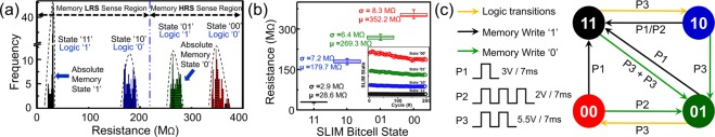
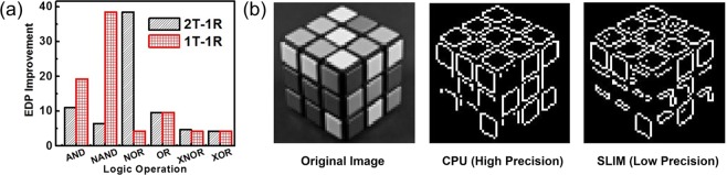
von Neumann architecture based computers isolate computation and storage (i.e. data is shuttled between computation blocks (processor) and memory blocks). The to-and-fro movement of data leads to a fundamental limitation of modern computers, known as the Memory wall. Logic in-Memory (LIM)/In-Memory Computing (IMC) approaches aim to address this bottleneck by directly computing inside memory units thereby eliminating energy-intensive and time-consuming data movement. Several recent works in literature, propose realization of logic function(s) directly using arrays of emerging resistive memory devices (example- memristors, RRAM/ReRAM, PCM, CBRAM, OxRAM, STT-MRAM etc.), rather than using conventional transistors for computing. The logic/embedded-side of digital systems (like processors, micro-controllers) can greatly benefit from such LIM realizations. However, the pure storage-side of digital systems (example SSDs, enterprise storage etc.) will not benefit much from such LIM approaches as when memory arrays are used for logic they lose their core functionality of storage. Thus, there is the need for an approach complementary to existing LIM techniques, that's more beneficial for the storage-side of digital systems; one that gives compute capability to memory arrays not at the cost of their existing stored states. Fundamentally, this would require memory nanodevice arrays that are capable of storing and computing simultaneously. In this paper, we propose a novel 'Simultaneous Logic in-Memory' (SLIM) methodology which is complementary to existing LIM approaches in literature. Through extensive experiments we demonstrate novel SLIM bitcells (1T-1R/2T-1R) comprising non-filamentary bilayer analog OxRAM devices with NMOS transistors. Proposed bitcells are capable of implementing both Memory and Logic operations simultaneously. Detailed programming scheme, array level implementation, and controller architecture are also proposed. Furthermore, to study the impact of proposed SLIM approach for real-world implementations, we performed analysis for two applications: (i) Sobel Edge Detection, and (ii) Binary Neural Network- Multi layer Perceptron (BNN-MLP). By performing all computations in SLIM bitcell array, huge Energy Delay Product (EDP) savings of ≈75× for 1T-1R (≈40× for 2T-1R) SLIM bitcell were observed for edge-detection application while EDP savings of ≈3.5× for 1T-1R (≈1.6× for 2T-1R) SLIM bitcell were observed for BNN-MLP application respectively, in comparison to conventional computing. EDP savings owing to reduction in data transfer between CPU ↔ memory is observed to be ≈780× (for both SLIM bitcells).


Conflict of interest statement

The authors declare no competing interests.

Figures

Figure 1
Figure 1
(a) von Neumann architecture with separate processing and memory units, LIM: memory blocks can perform logic, and SLIM: all memory blocks capable to perform Storage and Logic operations simultaneously and non-destructively, (b) Ideal computing system with LIM/SLIM co-existing with von Neumann CPU, enabling computation at all levels of memory hierarchy.
Figure 2
Figure 2
(a,b) HR-TEM and DC IV curve of bilayer Ni/HfO2/ATO/TiN OxRAM device, fabricated for this study (inset shows quite stable repeatable switching for 30 cycles) (c) Proposed circuit schematic of 1T-1R/2T-1R SLIM bitcell.
Figure 3
Figure 3
(a) SLIM state assignments for Logic and Memory operation. Note Memory LRS and HRS sense regions. Histograms show resistance distributions for 4 selected SLIM states on 1T-1R/2T-1R SLIM bitcell (>100 trials). (b) Resistance distribution for 4 selected SLIM states. Inset shows endurance for states: ‘11’, ‘10’, ‘01’, ‘00’ for 200 cycles. (c) Proposed SLIM programming signals and Memory-Logic state transitions for 1T-1R/2T-1R SLIM bitcell. All further SLIM operations use P1/P2/P3 pulses at V1/V2.
Figure 4
Figure 4
(a) Applied example signals for Memory Write ‘1’ and Memory Write ‘0’. Read conditions are specified in brackets.[All pulse duration = 7 ms] (b) Experimental measurements for Memory Write ‘1’ operation (program device to state ‘11’) with device’s initial state as: (i) ‘10’, (ii) ‘01’, and (iii) ‘00’. Memory Write ‘0’ operation (program device to state ‘01’) with device’s initial state as (iv) ‘11’, (v) ‘10’ and (vi) ‘00’. Blue line: transient current through OxRAM device. Black line: P1/P2/P3 (applied signals). Black square: Initial resistance state, Red circle: Final resistance state post SLIM operation. Please note in (iv,v), the transient current through OxRAM device falls due to gradual increase in non-volatile resistance with application of successive reset pulses. Note: The current scale in (ivi) is varied for clear demonstration of gradual switching in the OxRAM device.
Figure 5
Figure 5
Four possible input operand combinations: (a) a = b = ‘0’; (b) a = ‘0’, b = ‘1’; (c) a = ‘1’, b = ‘0’; (d) a = b = ‘1’; corresponding to NAND truth table and proposed signal mapping for each case for the 1T-1R SLIM bitcell. [VTB = VTE − VBE; operand a is mapped to VG = 10 V (7 ms long); operand b is mapped to V2 = P3 = 5.5 V (7 ms long)]. Experimental results for NAND logic implemented using 1T-1R SLIM bitcell with device’s initial state: ‘11’ (eh), and ‘01’ (il). Among the four operand combinations, OxRAM device switches to Logic HRS state (‘10’ or ‘00’) only for a = b = ‘1’. Blue: transient current through OxRAM device.
Algorithm 1
Algorithm 1
Algorithm for n × n SLIM bitcell array Refresh.
Figure 6
Figure 6
Four possible input operand combinations: (a) a = b = ‘0’; (b) a = ‘0’, b = ‘1’; (c) a = ‘1’, b = ‘0’; (d) a = b = ‘1’; corresponding to NOR truth table and proposed signal mapping for each case for the 2T-1R SLIM bitcell. [VTB = VTE − VBE; VG = 10 V (7 ms long); V2 = P3 = 5.5 V (7 ms long). Experimental results for NOR logic implemented using 2T-1R SLIM bitcell with device’s initial state: ‘11’ (eh), and ‘01’ (il). Among the four operand combinations, OxRAM device switches to Logic HRS state (‘10’ or ‘00’) for a = ‘0’, b = ‘1’; a = ‘1’, b = ‘0’ and a = b = ‘1’. Blue: transient current through OxRAM device. Black line: P3 in all cases (applied signal).
Figure 7
Figure 7
(a) Flowcharts for SLIM: Memory Write operation and Logic operations. Intelligent read is performed in both operations. Refresh scheme is an internal part of Logic operation. (b) Optimized Refresh Scheme corresponding to multiple SLIM MATs (Matrices). Each SLIM MAT has 8 × 8 bits. 1 Tag register is allocated to each SLIM MAT to track row status. Within each Tag register, 1-bit corresponds to 1 row of 8 × 8 SLIM MAT. Tag Byte is initialized to zero once a fresh SLIM MAT is used. Once a row is used for Logic operation, tag bit corresponding to it, is set high. When the tag byte contain all ‘1’s, the Refresh block is triggered and it sends instruction to refresh the contents of complete SLIM MAT. After Refresh operation, all the SLIM bitcells in given SLIM MAT will have absolute Memory states (‘11’/‘01’).
Figure 8
Figure 8
(a) Block diagram of SLIM processing unit. Refresh block forms an internal part of the Logic operation block. User operands are passed first to the SLIM control unit. The control unit with other blocks maps Logic operations on the 1T-1R array. (b,c) Proposed sensing mechanism used for reading the SLIM bitcell state.
Figure 9
Figure 9
1-bit Full Adder operation mapping on 1T-1R SLIM bitcell array (NAND logic) using SLIM Operation Compiler. Here An, Bn indicate inputs, En indicates output of Logic operation. Black circles indicate input/output for the adder.
Figure 10
Figure 10
(a) EDP comparison for performing 64-bit Logic operations using SLIM array w.r.t. conventional CPU architecture (fetching operands from DRAM (DDR3)), (b) Edge-detection output of ‘CPU + DRAM’ (center) and ‘CPU + SLIM bitcell array’ (right) along with the original image (left). Image sources: (b) Original image shown on left is a resized and cropped version of “BW Rubik’s Cube” by Gerwin Sturm (https://www.flickr.com/photos/scarygami/5568844961), licensed under CC BY-SA 2.0 (https://creativecommons.org/licenses/by-sa/2.0/). Images in center and right are generated by performing edge detection).
Figure 11
Figure 11
(a) Mapping of operations (XNOR and POPCOUNT) over SLIM MATs with addition SRAM based POPCOUNT LUT modules. All Logic operations are mapped on independent bitcells, considering no bitcell is reused during one inference cycle. Mapping ensures proximity for bitcells performing the same type of operation in the same layer. (b) Flowchart of SLIM-BNN computation. Since binary weight used for XNOR computation are [0, 1] rather than [−1, 1], a fixed offset has been subtracted in order to compute the same dot product.

References

    1. Wulf WA, McKee SA. Hitting the memory wall: implications of the obvious. ACM SIGARCH computer architecture news. 1995;23:20–24. doi: 10.1145/216585.216588. - DOI
    1. Horowitz, M. 1.1 computing’s energy problem (and what we can do about it). In Solid-State Circuits Conference Digest of Technical Papers (ISSCC), 2014 IEEE International, 10–14 (IEEE, 2014).
    1. Milojicic, D. et al. Computing in-memory, revisited. In 2018 IEEE 38th International Conference on Distributed Computing Systems (ICDCS), 1300–1309, 10.1109/ICDCS.2018.00130 (2018).
    1. Hennessy, J. L. & Patterson, D. A. Computer architecture: a quantitative approach (Elsevier, 2011).
    1. Chen Y-H, Krishna T, Emer JS, Sze V. Eyeriss: An energy-efficient reconfigurable accelerator for deep convolutional neural networks. IEEE Journal of Solid-State Circuits. 2017;52:127–138. doi: 10.1109/JSSC.2016.2616357. - DOI

Publication types