. 2020 Feb 7;6(6):eaax1425.
doi: 10.1126/sciadv.aax1425. eCollection 2020 Feb.

A hybrid quantum memory-enabled network at room temperature

Affiliations

A hybrid quantum memory-enabled network at room temperature

Xiao-Ling Pang et al. Sci Adv. .

Abstract

Quantum memory capable of storage and retrieval of flying photons on demand is crucial for developing quantum information technologies. However, the devices needed for long-distance links are different from those envisioned for local processing. We present the first hybrid quantum memory-enabled network by demonstrating the interconnection and simultaneous operation of two types of quantum memory: an atomic ensemble-based memory and an all-optical Loop memory. Interfacing the quantum memories at room temperature, we observe a well-preserved quantum correlation and a violation of Cauchy-Schwarz inequality. Furthermore, we demonstrate the creation and storage of a fully-operable heralded photon chain state that can achieve memory-built-in combining, swapping, splitting, tuning, and chopping single photons in a chain temporally. Such a quantum network allows atomic excitations to be generated, stored, and converted to broadband photons, which are then transferred to the next node, stored, and faithfully retrieved, all at high speed and in a programmable fashion.


Figures

Fig. 1
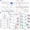
Fig. 1. A schematic diagram and experimental setup for a hybrid quantum memory enabled network.
(A) A quantum network consists of two different functional nodes and their interconnections. (B) Write and read processes of FORD quantum memory. Solid lines represent three-level Λ-type configuration of atoms, in which states ∣g⟩ and ∣s⟩ are hyperfine ground states of cesium atoms (Δs = 9.2 GHz); state ∣e⟩ is the excited state; dashed lines represent broad virtual energy levels induced by the write and read pulses. (C) Setup of FORD quantum memory. WP, Wollaston prism; PBS, polarization beam splitter; QWP, quarter wave plate; HWP, half wave plate. (D) Time sequences of FORD quantum memory. (E) Polarization switching in the mapping in-and-out processes shown in Bloch spheres. (F) Setup of Loop quantum memory. The Pockels cell in the loop is controlled by write and read electrical signals from two channels of a field-programmable gate array (FPGA) module. A 500-m-long fiber is introduced to coordinate with the Loop memory as another switching path against photon loss. Four avalanche photodiodes (APDs) are used to detect photons in a chain with small time interval. PC, Pockels cells. (G) Time sequences of Loop memory. The time interval τ2 between write and read signals can be any positive integral multiples of 1 cycle period τ.
Fig. 2
Fig. 2. Retrieval efficiency of FORD and loop memory.
(A) Retrieved distribution of anti-Stokes photons triggered by Stokes photons as a function of τ1. (C) Retrieved distribution of injected photons as a function of τ2 with the circulation period τ being 10.4 ns. (B and D) The red solid lines fit the measured retrieval efficiency of the FORD and Loop memories. Insets show the pulses at τ1 = 600 ns and τ2 = 114.4 ns with Gaussian fits, giving the duration of the retrieved broadband pulses. Comparing with the duration of 1.6 ns measured before the Loop memory, the pulse shape is well preserved. The transmission per round trip is 90% (two Pockels cell are used in the loop with the same clock rate of 50 kHz and a rise time of 5 ns, and the transmittance for each Pockels cell is 97%).
Fig. 3
Fig. 3. Measured cross-correlation as a function of storage time.
(A) The cross-correlation gS-AS(2)(τ1,τ2=31.2ns) is fitted with form gS-AS(2)(τ1)=1+C/(1+Aτ1+Bτ12), where the quadratic term describes atomic motion, and the linear term comes from background noise. (B) The cross-correlation gS-AS(2)(τ1=30ns,τ2) is fitted with form gS-AS(2)(τ2)=AeBτ2, which follows the exponential decay of the memory efficiency. The data are obtained under the condition of a write/read beam waist being 214 μm and the detuning ΔR = 4 GHz. Error bars are derived assuming Poissonian statistics of the individual photocounts. (C) Joint cross-correlation of the hybrid quantum memory–enabled network as a function of storage times. The surface is well described by the product of the two decay functions. The inset provides a top view of the measured points.
Fig. 4
Fig. 4. Experimental creation and storage of a fully operable heralded photon chain state.
(A) Schematic diagram of creating a two-photon chain with tunable interval and mapping the chain in and out to various temporal modes. t1 is the storage time of FORD memory, t2 is the time interval between two heralded anti-Stokes photons (AS1 and AS2), t3 is the interval between AS1 and AS2 after a 500-m fiber and two Pockels cells, t4 represents the interval between AS1(AS2) and the first part of AS2(AS1), and t5 is the interval between two chopped parts. The circulation period τ here is 20.3 ns, where the transmission rate of the Pockels cell in the loop is 95% with a clock rate of 30 MHz and a rise time of 5 ns. (B) Various temporal modes of anti-Stokes photons are marked in different colors. Heralded photons can be mapped out of the Loop memory to arbitrary temporal modes defined. The transmission rate of anti-Stokes photons between two memories is around 12.4%. FIFO, First in first out; FILO, first in last out. (C) Fine tuning of the mapped-out photons with a step of 2 ns. The inset portrays the shape of the mapped-out anti-Stokes photons. (D) Demonstration of chopping a single photon in a chain, where the probability is continuously tunable by adjusting half-wave voltage of the Pockels cell in the loop. The pulse shadows represent the sum of AS1(AS2) and AS1′(AS2′). Inserted bar graphs are measured cross-correlation values. More detailed values from t1 to t5 and cross-correlations can be found in the Supplementary Materials.

References

    1. O’Brien J. L., Furusawa A., Vučković J., Photonic quantum technologies. Nat. Photonics 3, 687–695 (2009).
    1. Jin X.-M., Ren J.-G., Yang B., Yi Z.-H., Zhou F., Xu X.-F., Wang S.-K., Yang D., Hu Y.-F., Jiang S., Yang T., Yin H., Chen K., Peng C.-Z., Pan J.-W., Experimental free-space quantum teleportation. Nat. Photonics 4, 376–381 (2010).
    1. Gisin N., Thew R., Quantum communication. Nat. Photonics 1, 165–171 (2007).
    1. Ladd T. D., Jelezko F., Laflamme R., Nakamura Y., Monroe C., OBrien J. L., Quantum computers. Nature 464, 45–53 (2010). - PubMed
    1. Aspuru-Guzik A., Walther P., Photonic quantum simulators. Nat. Phys. 8, 285–291 (2012).

LinkOut - more resources