. 2020 Feb 24;10(1):3236.
doi: 10.1038/s41598-020-60037-y.

Film-thickness-driven superconductor to insulator transition in cuprate superconductors

Affiliations

Film-thickness-driven superconductor to insulator transition in cuprate superconductors

Han-Byul Jang et al. Sci Rep. .

Abstract

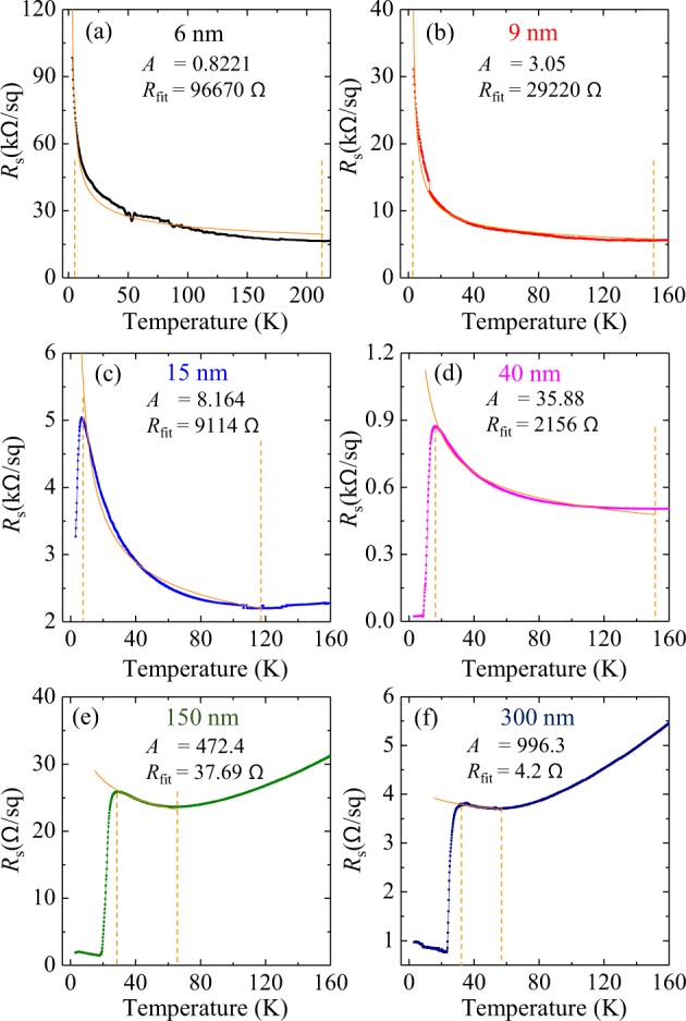
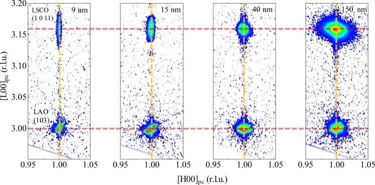
The superconductor-insulator transition induced by film thickness control is investigated for the optimally doped cuprate superconductor La1.85Sr0.15CuO4. Epitaxial thin films are grown on an almost exactly matched substrate LaAlO3 (001). Despite the wide thickness range of 6 nm to 300 nm, all films are grown coherently without significant relaxation of the misfit strain. Electronic transport measurement exhibits systematic suppression of the superconducting phase by reducing the film thickness, thereby inducing a superconductor-insulator transition at a critical thickness of ~10 nm. The emergence of a resistance peak preceding the superconducting transition is discussed based on the weak localization. X-ray photoelectron spectroscopy results show the possibility that oxygen vacancies are present near the interface.


Conflict of interest statement

The authors declare no competing interests.

Figures

Figure 1
Figure 1
(a) Temperature dependence of sheet resistance Rs for La1.85Sr0.15CuO4 thin films with film thicknesses of 6, 9, 15, 40, ~150 and ~300 nm. (b) The magnified linear-scale Rs − T curve of the 40-nm-thick film. The onset superconducting transition temperature is defined by the crossing point of two yellow extrapolated lines. The midpoint temperature is defined as the temperature at which resistance becomes half of the resistance at the onset temperature relative to the base resistance. (c) Superconducting transition temperatures versus logarithmic film thickness. The horizontal solid (dashed) line indicates the onset (midpoint) transition of the bulk target. (d) Semi-logarithmic Rs − T plot for the 40-nm-thick film. The labels of (i) to (iv) represent four conduction regimes that correspond to the metal, insulator, transition, and superconductor.
Figure 2
Figure 2
Theoretical fitting to the resistance peak for (a) 6 nm (b) 9 nm (c) 15 nm (d) 40 nm (e) ~150 nm and (f) ~300 nm thick films. The parameters A and Rfit were determined for each film thickness by fitting the theoretical curve (orange solid line) associated with the weak localization and interaction in a diffusion channel to the experimental data (square symbols) in the temperature range indicated by the two vertical dashed lines.
Figure 3
Figure 3
Crystal structural characterization by x-ray diffraction. (a) X-ray 2θ − ω scans for La1.85Sr0.15CuO4 thin films on LaAlO3 substrate. Black circles represent the peaks of LaAlO3 substrate. Vertical orange dashed lines exhibit the peak positions of the La1.85Sr0.15CuO4 films were almost identical regardless of different film thicknesses. (b) c-axis lattice parameter versus logarithmic film thickness. Error bar was evaluated from the FWHM of (006) peak. (c) The enlarged 2θ − ω scans for (006) peaks. The thicknesses of films thinner than 100 nm were defined by the Kiessig fringes and/or the Scherrer formula, while the two thickest films were estimated by growth time.
Figure 4
Figure 4
Reciprocal space maps of (1 0 11) film peak near (103) substrate peak for four different thick films. Reciprocal lattice unit (r.l.u.) is defined as 2π divided by the pseudocubic lattice parameter (3.789 Å) of LaAlO3 substrate. In-plane lattice parameters of the films exactly match with those of substrates, indicating fully strained films regardless of the different thicknesses. Out-of-plane lattice parameters are also almost same as a result of no significant strain relaxation.
Figure 5
Figure 5
Surface topographic images for the thickness-series of samples. Granularity is observed in all the samples. The typical grain size doesn’t show a correlation with film thickness. The two thickest samples (~150 nm and ~300 nm) exhibit significantly higher surface roughness than the others.
Figure 6
Figure 6
High-angle annular dark-field (HAADF) image of a La1.85Sr0.15CuO4 thin film. (a) A large area image of the film and substrate. (b) High-resolution image of the interfacial area between the thin film and the substrate. (c) The epitaxial relation between film and substrate at the interface. It can be also clearly seen that the thin film has a layered perovskite structure.
Figure 7
Figure 7
Core level XPS spectrum for 6, 9, 15, and 40-nm-thick films with 0.05 eV step size. (a) Core level Cu 2p3/2 XPS spectra. The main and suppressed satellite peaks correspond to 2p3d10L-like and 2p3d9-like states, respectively. Yellow guide line indicates the peak centers of 2p3d10L-like states. (b) O 1 s core XPS spectra. The yellow guide lines indicate the peak centers of O 1 s peaks. Wine dashed line indicates the surface hydroxide peaks. (c) Binding energy shifts of O 1 s and Cu 2p3/2 core levels relative to those of the 6-nm-thick film. Error bar represents a measurement step of ±0.025 eV.

References

    1. Hsu S-Y, Valles JM. Magnetic-field-induced pair-breaking effects in granular Pb films near the superconductor-to-insulator transition. Phys. Rev. B. 1993;48:4164–4167. doi: 10.1103/PhysRevB.48.4164. - DOI - PubMed
    1. Crassous A, et al. Nanoscale electrostatic manipulation of magnetic flux quanta in ferroelectric/superconductor BiFeO3/YBa2Cu3O7−δ heterostructures. Phys. Rev. Lett. 2011;107:247002. doi: 10.1103/PhysRevLett.107.247002. - DOI - PubMed
    1. Bollinger AT, et al. Superconductor-insulator transition in La2- xSrxCuO4 at the pair quantum resistance. Nature. 2011;472:458–460. doi: 10.1038/nature09998. - DOI - PubMed
    1. Ye JT, et al. Liquid-gated interface superconductivity on an atomically flat film. Nat. Mater. 2010;9:125–128. doi: 10.1038/nmat2587. - DOI - PubMed
    1. Ueno K, et al. Electric-field-induced superconductivity in an insulator. Nat. Mater. 2008;7:855–858. doi: 10.1038/nmat2298. - DOI - PubMed