

Flexibility of Fluorinated Graphene-Based Materials
- PMID: 32106413
- PMCID: PMC7084608
- DOI: 10.3390/ma13051032
Flexibility of Fluorinated Graphene-Based Materials
Abstract
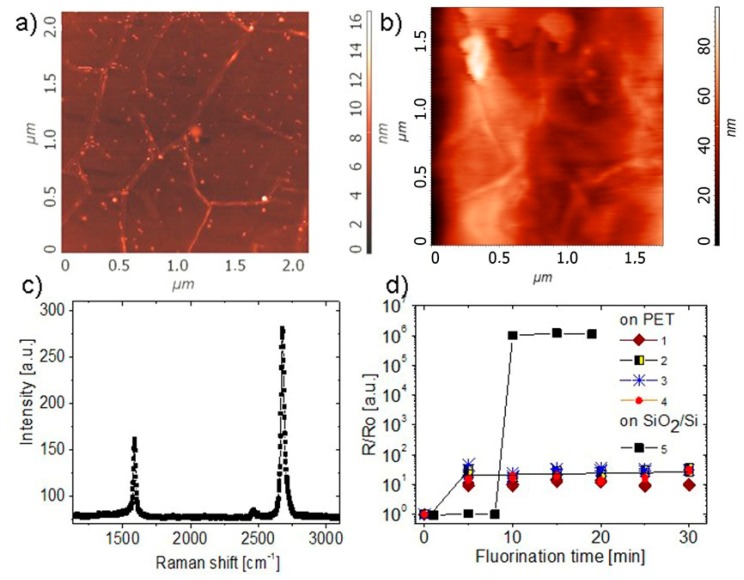
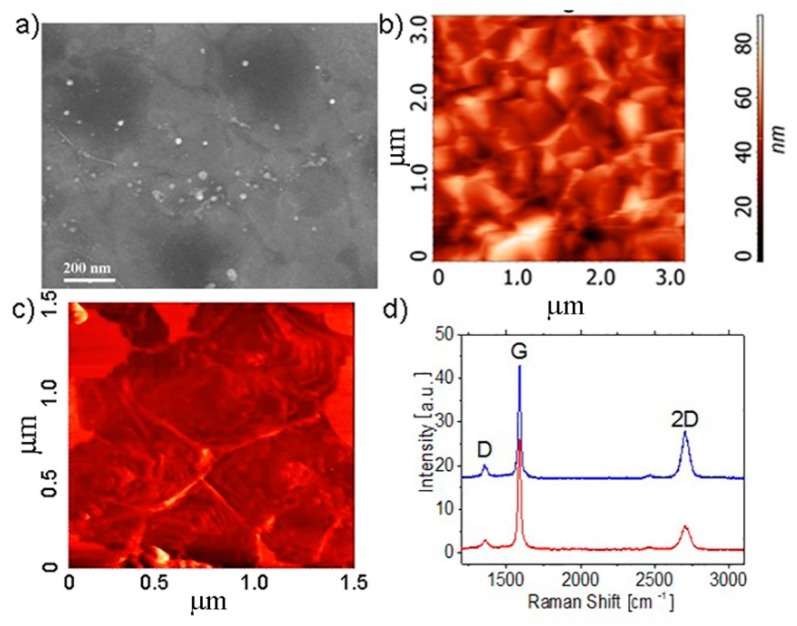
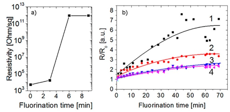
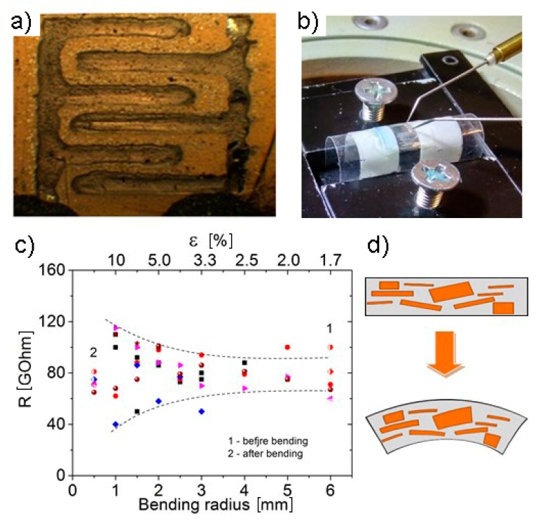
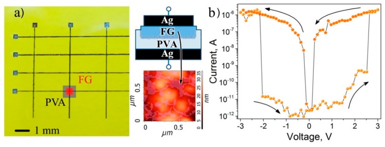
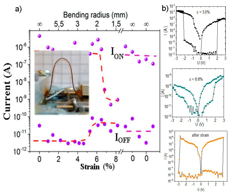
The resistivity of different films and structures containing fluorinated graphene (FG) flakes and chemical vapor deposition (CVD)-grown graphene of various fluorination degrees under tensile and compressive strains due to bending deformations was studied. Graphene and multilayer graphene films grown by means of the chemical vapor deposition (CVD) method were transferred onto the flexible substrate by laminating and were subjected to fluorination. They demonstrated a weak fluorination degree (F/C lower 20%). Compressive strains led to a strong (one-two orders of magnitude) decrease in the resistivity in both cases, which was most likely connected with the formation of additional conductive paths through fluorinated graphene. Tensile strain up to 3% caused by the bending of both types of CVD-grown FG led to a constant value of the resistivity or to an irreversible increase in the resistivity under repeated strain cycles. FG films created from the suspension of the fluorinated graphene with a fluorination degree of 20-25%, after the exclusion of design details of the used structures, demonstrated a stable resistivity at least up to 2-3% of tensile and compressive strain. The scale of resistance changes R/R0 was found to be in the range of 14-28% with a different sign at the 10% tensile strain (bending radius 1 mm). In the case of the structures with the FG thin film printed on polyvinyl alcohol, a stable bipolar resistive switching was observed up to 6.5% of the tensile strain (bending radius was 2 mm). A further increase in strain (6.5-8%) leads to a decrease in ON/OFF current ratio from 5 down to 2 orders of magnitude. The current ratio decrease is connected with an increase under the tensile strain in distances between conductive agents (graphene islands and traps at the interface with polyvinyl alcohol) and thickness of fluorinated barriers within the active layer. The excellent performance of the crossbar memristor structures under tensile strain shows that the FG films and structures created from suspension are especially promising for flexible electronics.
Keywords: CVD-grown graphene; FG suspension; fluorinated graphene; resistive switching; resistivity; tensile and compressive strains.
Conflict of interest statement
The authors declare no conflict of interest.
Figures

Similar articles
-
Resistive switching effects in fluorinated graphene films with graphene quantum dots enhanced by polyvinyl alcohol.Nanotechnology. 2019 Jun 21;30(25):255701. doi: 10.1088/1361-6528/ab0cb3. Epub 2019 Mar 5. Nanotechnology. 2019. PMID: 30836347
-
Fluorination of graphene: a spectroscopic and microscopic study.ACS Nano. 2014 Feb 25;8(2):1862-70. doi: 10.1021/nn406333f. Epub 2014 Feb 4. ACS Nano. 2014. PMID: 24471932
-
Two-layer and composite films based on oxidized and fluorinated graphene.Phys Chem Chem Phys. 2017 Jul 26;19(29):19010-19020. doi: 10.1039/c7cp03609d. Phys Chem Chem Phys. 2017. PMID: 28702590
-
Memristive FG-PVA Structures Fabricated with the Use of High Energy Xe Ion Irradiation.Materials (Basel). 2022 Mar 11;15(6):2085. doi: 10.3390/ma15062085. Materials (Basel). 2022. PMID: 35329539 Free PMC article.
-
Recent Advances in Fluorinated Graphene from Synthesis to Applications: Critical Review on Functional Chemistry and Structure Engineering.Adv Mater. 2022 Jan;34(1):e2101665. doi: 10.1002/adma.202101665. Epub 2021 Oct 17. Adv Mater. 2022. PMID: 34658081 Review.
Cited by
-
Large Deflection Analysis of Peripherally Fixed Circular Membranes Subjected to Liquid Weight Loading: A Refined Design Theory of Membrane Deflection-Based Rain Gauges.Materials (Basel). 2021 Oct 12;14(20):5992. doi: 10.3390/ma14205992. Materials (Basel). 2021. PMID: 34683584 Free PMC article.
-
Ab Initio Insight into the Interaction of Metal-Decorated Fluorinated Carbon Fullerenes with Anti-COVID Drugs.Int J Mol Sci. 2022 Feb 21;23(4):2345. doi: 10.3390/ijms23042345. Int J Mol Sci. 2022. PMID: 35216462 Free PMC article.
-
Graphene Flakes for Electronic Applications: DC Plasma Jet-Assisted Synthesis.Nanomaterials (Basel). 2020 Oct 16;10(10):2050. doi: 10.3390/nano10102050. Nanomaterials (Basel). 2020. PMID: 33081370 Free PMC article.
-
Fluorescent Submicron-Sized Poly(heptafluoro-n-butyl methacrylate) Particles with Long-Term Stability.Molecules. 2020 Apr 25;25(9):2013. doi: 10.3390/molecules25092013. Molecules. 2020. PMID: 32344920 Free PMC article.
References
-
- Zhu W., Park S., Yogeesh M., Akinwande D. Advancements in 2D flexible nanoelectronics: From material perspectives to RF applications. Flex. Print. Electron. 2017;2:043001. doi: 10.1088/2058-8585/aa84a4. - DOI
-
- Chen G., Zhang P., Pan L., Qi L., Yu F., Gao C. Flexible nonvolatile resistive memory devices based on SrTiO3 nanosheets and polyvinylpyrrolidone composites. J. Mater. Chem. C. 2017;5:9799. doi: 10.1039/C7TC03481D. - DOI
LinkOut - more resources
Full Text Sources
Miscellaneous
