

Femtosecond Transient Absorption Microscopy of Singlet Exciton Motion in Side-Chain Engineered Perylene-Diimide Thin Films
- PMID: 32130861
- PMCID: PMC7132576
- DOI: 10.1021/acs.jpca.0c00346
Femtosecond Transient Absorption Microscopy of Singlet Exciton Motion in Side-Chain Engineered Perylene-Diimide Thin Films
Abstract
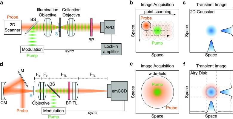
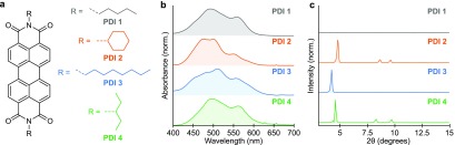
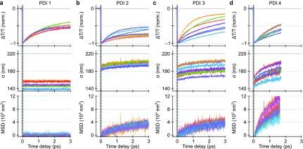
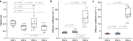
We present a statistical analysis of femtosecond transient absorption microscopy applied to four different organic semiconductor thin films based on perylene-diimide (PDI). By achieving a temporal resolution of 12 fs with simultaneous sub-10 nm spatial precision, we directly probe the underlying exciton transport characteristics within 3 ps after photoexcitation free of model assumptions. Our study reveals sub-picosecond coherent exciton transport (12-45 cm2 s-1) followed by a diffusive phase of exciton transport (3-17 cm2 s-1). A comparison between the different films suggests that the exciton transport in the studied materials is intricately linked to their nanoscale morphology, with PDI films that form large crystalline domains exhibiting the largest diffusion coefficients and transport lengths. Our study demonstrates the advantages of directly studying ultrafast transport properties at the nanometer length scale and highlights the need to examine nanoscale morphology when investigating exciton transport in organic as well as inorganic semiconductors.
Conflict of interest statement
The authors declare no competing financial interest.
Figures
Similar articles
-
Direct Imaging of Frenkel Exciton Transport by Ultrafast Microscopy.Acc Chem Res. 2017 Jul 18;50(7):1725-1733. doi: 10.1021/acs.accounts.7b00155. Epub 2017 Jul 5. Acc Chem Res. 2017. PMID: 28678469
-
Morphology-Independent Efficient Singlet Exciton Fission in Perylene Diimide Thin Films.Chempluschem. 2018 Apr;83(4):230-238. doi: 10.1002/cplu.201700449. Epub 2018 Feb 9. Chempluschem. 2018. PMID: 31957287
-
Self-trapping limited exciton diffusion in a monomeric perylene crystal as revealed by femtosecond transient absorption microscopy.Phys Chem Chem Phys. 2008 Aug 14;10(30):4435-41. doi: 10.1039/b801856a. Epub 2008 Jun 6. Phys Chem Chem Phys. 2008. PMID: 18654683
-
Exciton diffusion in organic semiconductors: precision and pitfalls.Nanoscale. 2024 Oct 3;16(38):17761-17777. doi: 10.1039/d4nr02467b. Nanoscale. 2024. PMID: 39171513 Review.
-
Transient Absorption Spectroscopy of Films: Impact of Refractive Index.J Phys Chem C Nanomater Interfaces. 2024 Apr 5;128(15):6167-6179. doi: 10.1021/acs.jpcc.4c00981. eCollection 2024 Apr 18. J Phys Chem C Nanomater Interfaces. 2024. PMID: 38655057 Free PMC article. Review.
Cited by
-
Rapid Exciton Transport and Structural Defects in Individual Porphyrinic Metal Organic Framework Microcrystals.J Am Chem Soc. 2024 Feb 21;146(7):4309-4313. doi: 10.1021/jacs.3c12275. Epub 2024 Feb 8. J Am Chem Soc. 2024. PMID: 38330249 Free PMC article.
-
A New Frontier in Exciton Transport: Transient Delocalization.J Phys Chem Lett. 2022 Jul 28;13(29):6820-6830. doi: 10.1021/acs.jpclett.2c01133. Epub 2022 Jul 20. J Phys Chem Lett. 2022. PMID: 35857739 Free PMC article. Review.
-
Exciton transport in molecular organic semiconductors boosted by transient quantum delocalization.Nat Commun. 2022 May 19;13(1):2755. doi: 10.1038/s41467-022-30308-5. Nat Commun. 2022. PMID: 35589694 Free PMC article.
-
Leaving the Limits of Linearity for Light Microscopy.J Phys Chem C Nanomater Interfaces. 2020 Nov 12;124(45):24555-24565. doi: 10.1021/acs.jpcc.0c07501. Epub 2020 Sep 22. J Phys Chem C Nanomater Interfaces. 2020. PMID: 34306294 Free PMC article.
-
Progress and Prospects in Optical Ultrafast Microscopy in the Visible Spectral Region: Transient Absorption and Two-Dimensional Microscopy.J Phys Chem C Nanomater Interfaces. 2023 Jul 24;127(30):14557-14586. doi: 10.1021/acs.jpcc.3c02091. eCollection 2023 Aug 3. J Phys Chem C Nanomater Interfaces. 2023. PMID: 37554548 Free PMC article. Review.
References
-
- Yu G.; Gao J.; Hummelen J. C.; Wudl F.; Heeger A. J. Polymer Photovoltaic Cells: Enhanced Efficiencies via a Network of Internal Donor-Acceptor Heterojunctions. Science (Washington, DC, U. S.) 1995, 270 (5243), 1789–1791. 10.1126/science.270.5243.1789. - DOI
-
- Hendsbee A. D.; Sun J. P.; Law W. K.; Yan H.; Hill I. G.; Spasyuk D. M.; Welch G. C. Synthesis, Self-Assembly, and Solar Cell Performance of N-Annulated Perylene Diimide Non-Fullerene Acceptors. Chem. Mater. 2016, 28 (19), 7098–7109. 10.1021/acs.chemmater.6b03292. - DOI
LinkOut - more resources
Full Text Sources
