. 2020 Mar 24;14(3):3316-3327.
doi: 10.1021/acsnano.9b08943. Epub 2020 Mar 12.

Atomic-Scale Patterning of Arsenic in Silicon by Scanning Tunneling Microscopy

Affiliations

Atomic-Scale Patterning of Arsenic in Silicon by Scanning Tunneling Microscopy

Taylor J Z Stock et al. ACS Nano. .

Abstract

Over the past two decades, prototype devices for future classical and quantum computing technologies have been fabricated by using scanning tunneling microscopy and hydrogen resist lithography to position phosphorus atoms in silicon with atomic-scale precision. Despite these successes, phosphine remains the only donor precursor molecule to have been demonstrated as compatible with the hydrogen resist lithography technique. The potential benefits of atomic-scale placement of alternative dopant species have, until now, remained unexplored. In this work, we demonstrate the successful fabrication of atomic-scale structures of arsenic-in-silicon. Using a scanning tunneling microscope tip, we pattern a monolayer hydrogen mask to selectively place arsenic atoms on the Si(001) surface using arsine as the precursor molecule. We fully elucidate the surface chemistry and reaction pathways of arsine on Si(001), revealing significant differences to phosphine. We explain how these differences result in enhanced surface immobilization and in-plane confinement of arsenic compared to phosphorus, and a dose-rate independent arsenic saturation density of 0.24 ± 0.04 monolayers. We demonstrate the successful encapsulation of arsenic delta-layers using silicon molecular beam epitaxy, and find electrical characteristics that are competitive with equivalent structures fabricated with phosphorus. Arsenic delta-layers are also found to offer confinement as good as similarly prepared phosphorus layers, while still retaining >80% carrier activation and sheet resistances of <2 kΩ/square. These excellent characteristics of arsenic represent opportunities to enhance existing capabilities of atomic-scale fabrication of dopant structures in silicon, and may be important for three-dimensional devices, where vertical control of the position of device components is critical.

Keywords: arsenic; arsine; atomic fabrication; density functional theory; dopant; scanning tunneling microscopy; silicon (001).


Conflict of interest statement

The authors declare no competing financial interest.

Figures

Figure 1
Figure 1
Adsorption and dissociation of single AsH3 molecules on Si(001)2 × 1. (a,b) Filled and empty state STM images of low-coverage AsH3 on Si(001). AsH3 features are labeled type-1 and type-2, native surface defects are dimer vacancies (DV), double dimer vacancy (2DV), 2 + 1 dimer vacancy complex (2 + 1DV), and C-defect (Cd). Sample voltage, V = −1.7 V, +1.6 V; tunneling current, I = 0.10 nA. (c) Filled-state STM image of a type-1 feature. Reticle highlights alignment with Si dimers. V = −1.7 V, I = 0.10 nA. (d) Schematic valence diagram details the inter-row end-bridge As + 3H structure of the type-1 feature. Gray shading indicates regions imaging bright in STM. (e) Empty-state STM image of a type-1 feature. Reticles indicate the positions of Si dimers. V = +1.6 V, I = 0.10 nA. (f) Structural schematic of inter-row end-bridge As + 3H structure showing the positions of first and second layer silicon atoms (black and gray, respectively), and the single As (green) and three H atoms (blue) provided by the AsH3 molecule. (g) Five-step reaction path from molecularly adsorbed AsH3 to the fully dissociated inter-row end-bridge As + 3H structure. Calculated adsorption energies are provided in brackets for each sequential structure. Calculated activation energies, EA, for each step are given above the reaction arrows. The STM images are skewed to account for thermal drift and rotated ∼45° from the scan direction such that the dimer-rows align with the horizontal.
Figure 2
Figure 2
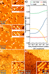
Substitutional incorporation of isolated arsenic atoms into the silicon lattice and saturation arsine coverage. (a) STM image of low coverage (0.02 adsorbates/nm2), room temperature AsH3 on Si(001). Arrows indicate examples of isolated type-1 AsH3 features. V = −1.7 V, I = 0.02 nA. The inset shows filled and empty state images of the type-1 feature alongside a C-defect for comparison. (b) Surface from panel (a) subsequent to a 500 °C × 1 min anneal. Isolated As–Si heterodimers (HD) are observed in the first layer of the silicon surface; examples are indicated by white arrows. V = −1.6 V, I = 0.10 nA. Two examples of the As–Si HD are shown in filled and empty states in the inset. (c) Kinetic Monte Carlo simulation of total As surface coverage and AsHx species distribution, as a function of arsine partial pressure. (d) STM image of a Si(001) surface following a 1.5 L (5 × 10⁻⁹ mbar × 5 min) room temperature, arsine exposure. Inset shows a magnified image of the same surface. V = −2.0 V, I = 0.04 nA. (e) Surface from panel (a) subsequent to a 350 °C × 1 min anneal. Inset shows ejected silicon dimer chains indicative of arsenic incorporation. V = −2.0 V, I = 0.05 nA.
Figure 3
Figure 3
Compatibility of AsH3 adsorption, dissociation, and incorporation with STM hydrogen resist lithography. (a–f) Sequential STM images of the same 100 × 100 nm area on a Si(001)-H surface showing that the H-resist remains intact and free from adsorbates throughout each step of the STM lithography process. (a) Clean hydrogen terminated Si(001) surface prior to STM lithography or arsine exposure. (b) Selected area hydrogen desorption of a 50 × 50 nm square (V = +7.0 V, I = 1 nA, s = 100 nm/s). (c) 1.5 L arsine dose results in selective adsorption only within the lithographically defined area. (d) 350 °C × 1 min anneal, results in incorporation of the adsorbed arsenic atoms as evidenced by presence of ejected Si. (e) Enlargement of the upper right-hand corner of the patterned square in panel (c). The disordered saturation arsenic layer is clearly contained within only the patterned region, and there is no adsorption on the resist. (f) Enlargement of the upper right-hand corner of the patterned square in panel (d). Short Si dimer chains, evidence of arsenic incorporation, are indicated by the arrows. The surrounding hydrogen resist remains essentially intact with only a small density of additional dangling bonds produced by the incorporation anneal. V = −2.0 V, I = 0.10 nA. (g) Sequential images of hydrogen desorption, AsH3 adsorption, and As incorporation along a line that is only 2 Si dimer rows wide. Arrows indicate a silicon dangling bond (DB) dimer, an adsorbed/dissociated AsHx moiety, and finally ejected silicon (ad-Si).
Figure 4
Figure 4
Arsenic δ-layer distribution and electronic transport controlled through a silicon overgrowth thermal annealing program. (a–e) SIMS profiles of five different saturation arsenic δ-layer samples overgrown with 15 nm Si, at a deposition rate of 1 ML/min. Sample temperature program during silicon epitaxy was modified for each sample according to the inset temperature vs time profiles. (f) δ-Layer mobility and confinement as a function of RTA temperature. (g) δ-Layer carrier density and sheet resistance as a function of RTA temperature. Error bars in the plots in panels f and g account for temperature measurement uncertainty and magnetoresistance curve fitting confidence levels as explained in the Supporting Information, section b.

References

    1. Jehl X.; Niquet Y. M.; Sanquer M. Single Donor Electronics and Quantum Functionalities with Advanced CMOS Technology. J. Phys.: Condens. Matter 2016, 28, 103001.10.1088/0953-8984/28/10/103001. - DOI - PubMed
    1. Morton J. J. L.; McCamey D. R.; Eriksson M. A.; Lyon S. A. Embracing the Quantum Limit in Silicon Computing. Nature 2011, 479, 345–353. 10.1038/nature10681. - DOI - PubMed
    1. Schofield S. R.; Curson N. J.; Simmons M. Y.; Rueß F. J.; Hallam T.; Oberbeck L.; Clark R. G. Atomically Precise Placement of Single Dopants in Si. Phys. Rev. Lett. 2003, 91, 136104.10.1103/PhysRevLett.91.136104. - DOI - PubMed
    1. Hudak B. M.; Song J.; Sims H.; Troparevsky M. C.; Humble T. S.; Pantelides S. T.; Snijders P. C.; Lupini A. R. Directed Atom-by-Atom Assembly of Dopants in Silicon. ACS Nano 2018, 12, 5873–5879. 10.1021/acsnano.8b02001. - DOI - PubMed
    1. Sinthiptharakoon K.; Schofield S. R.; Studer P.; Brázdová V.; Hirjibehedin C. F.; Bowler D. R.; Curson N. J. Investigating Individual Arsenic Dopant Atoms in Silicon Using Low-Temperature Scanning Tunnelling Microscopy. J. Phys.: Condens. Matter 2014, 26, 01200110.1088/0953-8984/26/1/012001. - DOI - PubMed