. 2020 Mar 4;20(5):1390.
doi: 10.3390/s20051390.

Automotive 3.0 µm Pixel High Dynamic Range Sensor with LED Flicker Mitigation

Affiliations

Automotive 3.0 µm Pixel High Dynamic Range Sensor with LED Flicker Mitigation

Minseok Oh et al. Sensors (Basel). .

Abstract

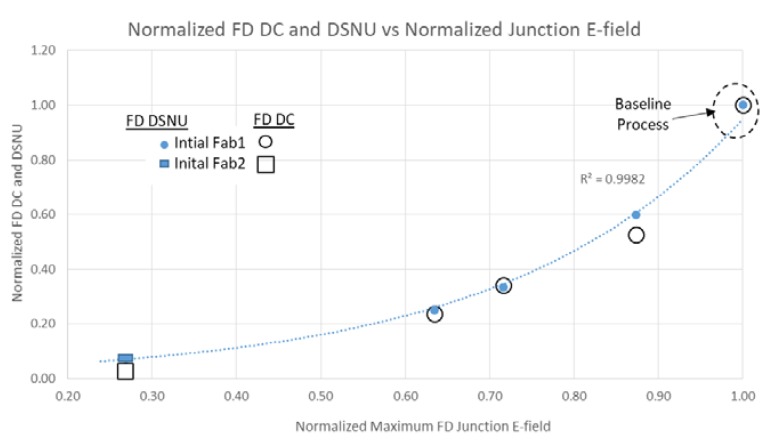
We present and discuss parameters of a high dynamic range (HDR) image sensor with LED flicker mitigation (LFM) operating in automotive temperature range. The total SNR (SNR including dark fixed pattern noise), of the sensor is degraded by floating diffusion (FD) dark current (DC) and dark signal non-uniformity (DSNU). We present results of FD DC and DSNU reduction, to provide required SNR versus signal level at temperatures up to 120 °C. Additionally we discuss temperature dependencies of quantum efficiency (QE), sensitivity, color effects, and other pixel parameters for backside illuminated image sensors. Comparing +120 °C junction vs. room temperature, in visual range we measured a few relative percent increase, while in 940 nm band range we measured 1.46x increase in sensitivity. Measured change of sensitivity for visual bands-such as blue, green, and red colors-reflected some impact to captured image color accuracy that created slight image color tint at high temperature. The tint is, however, hard to detect visually and may be removed by auto white balancing and temperature adjusted color correction matrixes.

Keywords: CMOS; LED flicker mitigation; automotive; high dynamic range; image sensor; quantum efficiency; sensitivity; temperature dependence.


Conflict of interest statement

The authors declare no conflict of interest.

Figures

Figure 1
Figure 1
(a) Pixel schematic; (b) Timing diagram.
Figure 2
Figure 2
(a) Signal vs. illuminance plot; (b) Total SNR vs. illuminance plot at 100 °C (T1: 16.6 ms and T2: 0.13 ms).
Figure 3
Figure 3
Images of E1 to E2 transition total SNR of (a) 32 dB, (b) 20 dB.
Figure 4
Figure 4
Sample HDR images in overflow (a), sequential (b), and overflow 100 °C, 33 ms tint (c) exposure modes.
Figure 5
Figure 5
(a) Waveform and parameters used for Monte Carlo simulation; (b) An example of Δφ distribution.
Figure 6
Figure 6
Simulation results of LED pulse detection probability vs. LED frequency vs. photoelectron generation rate.
Figure 7
Figure 7
Simulation results. (a) The mean of combined signal, (b) LED signal fluctuation, (c) LED frequency = 80 Hz, PGR = 1 × 10⁵ e/s, and (d) LED frequency = 80 Hz, PGR = 1 × 10⁶ e/s
Figure 8
Figure 8
FD DC and DSNU of initial processes vs. FD junction E-field.
Figure 9
Figure 9
PD DSNU vs. PD junction E-field.
Figure 10
Figure 10
PD DC vs. PD junction E-field.
Figure 11
Figure 11
FD DC vs. FD DSNU, both initial processes and new processes.
Figure 12
Figure 12
New process conditions FD DC and FD DSNU (measured vs. modeled).
Figure 13
Figure 13
DSNU vs. FD junction E-field for new process conditions and new layout.
Figure 14
Figure 14
FD dark current histograms.
Figure 15
Figure 15
Pixel simulation model.
Figure 16
Figure 16
Simulated Si absorption and quantum efficiency across different temperatures for pixel without µlens, CFA, and Si ARC.
Figure 17
Figure 17
Normalized measurement results of the SF gain across automotive temperature range.
Figure 18
Figure 18
Measurement results of the pixel transaction factor gains across automotive temperature range.
Figure 19
Figure 19
Relative light power spectral distributions and filter transmissions used for sensitivity extraction in visual and NIR ranges.
Figure 20
Figure 20
Measured normalized quantum efficiency change across different temperatures for 3 µm BSI Sensor 1.
Figure 21
Figure 21
Measured normalized quantum efficiency change across different temperatures for 2.2 µm BSI Sensor 2.
Figure 22
Figure 22
Normalized sensitivity change in visual (a) and NIR (b) ranges for both sensors.
Figure 23
Figure 23
Normalized color sensitivity change vs. temperature.
Figure 24
Figure 24
D65 and A-light R/G and B/G color ratio change vs. temperature.
Figure 25
Figure 25
Macbeth chart images and their corresponding color accuracy at room (left) and 120 °C junction (right) temperatures.

References

    1. Silsby C., Velichko S., Johnson S., Lim Y.P., Mentzer R., Beck J. A 1.2MP 1/3 CMOS Image Sensor with Light Flicker Mitigation; Proceedings of the IISW 2015; Vaals, The Netherlands. 8–11 June 2015.
    1. Velichko S., Johnson S., Pates D., Silsby C., Hoekstra C., Mentzer R., Beck J. 140dB Dynamic Range Sub-electron Noise Floor Image Sensor; Proceedings of the IISW 2017; Hiroshima, Japan. 30 May–2 June 2015.
    1. Iida S., Sakano Y., Asatsuma T., Takami M., Yoshiba I., Ohba N., Mizuno H., Oka T., Yamaguchi K., Suzuki A., et al. A 0.68e-rms random-noise 121dB dynamic-range sub-pixel architecture CMOS image sensor with LED flicker mitigation; Proceedings of the 2018 IEEE International Electron Devices Meeting (IEDM); San Francisco, CA, USA. 1–5 December 2018; pp. 221–224.
    1. Yu J., Collins D.J., Yasan A., Bae S., Ramaswami S. Hot Pixel reduction in CMOS image Sensor Pixels; Proceedings of the IS&T/SPIE Electronic Imaging; San Jose, CA, USA. 17–21 January 2010;
    1. Takahashi S., Huang Y.-M., Sze J.-J., Wu T.-T., Guo F.-S., Hsu W.-C., Tseng T.-H., Liao K., Kuo C.-C., Chen T.-H., et al. A 45nm Stacked CMOS Image Sensor Process Technology for Submicron Pixel. Sensors. 2017;17:2816. doi: 10.3390/s17122816. - DOI - PMC - PubMed

LinkOut - more resources