Review
. 2020 Mar 4;11(3):264.
doi: 10.3390/mi11030264.

Hybrid Polymer/Metal Oxide Thin Films for High Performance, Flexible Transistors

Affiliations
Review

Hybrid Polymer/Metal Oxide Thin Films for High Performance, Flexible Transistors

Jae Won Jeong et al. Micromachines (Basel). .

Abstract

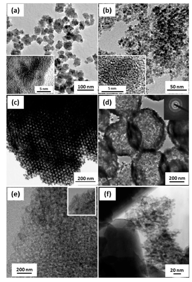
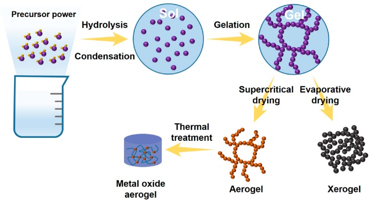
Metal oxides (MOs) have garnered significant attention in a variety of research fields, particularly in flexible electronics such as wearable devices, due to their superior electronic properties. Meanwhile, polymers exhibit excellent mechanical properties such as flexibility and durability, besides enabling economic solution-based fabrication. Therefore, MO/polymer nanocomposites are excellent electronic materials for use in flexible electronics owing to the confluence of the merits of their components. In this article, we review recent developments in the synthesis and fabrication techniques for MO/polymer nanocomposite-based flexible transistors. In particular, representative MO/polymer nanocomposites for flexible and transparent channel layers and gate dielectrics are introduced and their electronic properties-such as mobilities and dielectric constant-are presented. Finally, we highlight the advances in interface engineering and its influence on device electronics.

Keywords: active layers; dielectrics; flexible transistors; metal oxides; nanocomposites; polymers.


Conflict of interest statement

The authors declare no conflict of interest.

Figures

Figure 1
Figure 1
(af) A set of TEM images of diverse MO nanostructures: (a) MnO and (b) Fe3O4 nanoparticles fabricated via microwave-assisted synthesis (Reproduced from [42], Copyright 2008 Royal Society of Chemistry C), (c) porous SnO2 aerosols prepared via sol–gel method (reproduced with permission from [41], Copyright 2005 Wiley-VCH Verlag GmbH & Co. KGaA, Weinheim), (d) ZnO hollow spheres synthesized via hydrothermal synthesis (reproduced with permission from [40], Copyright 2008 American Chemical Society), (e) In2O3 nanoparticles prepared via anodization-precipitation (reproduced with permission from [37], Copyright 2018 American Chemical Society), and (f) TiO2 nanoparticle layer on SiO2 prepared via CVD, respectively (reproduced with permission from [43], Copyright 2001 Elsevier).
Figure 2
Figure 2
Reaction routes for the production of MO nanostructures by the sol–gel method.
Figure 3
Figure 3
(a) Schematic representation of the flexible, transparent TFT structure based on a metal oxide:polymer (In2O3: x% PVP) semiconductor blend. (b) X-ray diffraction (XRD) patterns of In2O3: polymer films with various PVP concentrations: annealing at 225 °C. (c) TFT mobility and threshold voltage for In2O3: polymer films having different PVP concentrations, processed at 225 °C. (d) Dependence of TFT mobilities on bending radius of both neat In2O3 TFTs and all-amorphous In2O3: 5% PVP TFTs (left), and mobilities on all-amorphous TFT bending cycles at a radius of 10 mm. Inset: Optical image of transparent flexible TFTs. Reproduced with permission from [91], Copyright 2015 Wiley-VCH Verlag GmbH & Co. KGaA, Weinheim.
Figure 4
Figure 4
(a) Chemical structure of PEI. (b) GIXRD patterns of In2O3: x% PEI blend films with differing PEI concentrations. (c) Derived coordination number, In-O bond lengths for the indicated films. (d) TFT mobility and threshold voltage for In2O3: x wt % PEI (250 °C), IZO: x wt % PEI, IGO: x wt % PEI, and IGZO: x wt % PEI, as a function of the polymer concentration. Tannealing = 300 °C. Reproduced with permission from [93], Copyright, 2016 Wiley-VCH Verlag GmbH & Co. KGaA, Weinheim.
Figure 5
Figure 5
(a) Schematic illustration of improved hydrophobicity of the IGZO: PTFE film. Transfer characteristics of (b) the IGZO TFT and (c) the IGZO: 20 W PTFE TFT upon exposure to water for different times. (d) Variations of mobility (μFE), on-current, and Vth for IGZO and IGZO: 20 W PTFE TFTs with respect to bending cycles. Reproduced permission from [95], Copyright, 2018, American Chemical Society.
Figure 6
Figure 6
(a) Optical microscopy images of In2O3 deposition (right to left) without PS, with PS1, with PS2, with PS3, and with PS4. The scale bar is 100 μm. (b) Transfer characteristics of inkjet-printed TFTs. (c) X-ray photoelectron spectroscopy (XPS) of O 1s spectra. Reproduced with permission from [96], Copyright 2018, American Institute of Physics.
Figure 7
Figure 7
(a) SEM image of the TFT cross section, where the PMMA−ZrO2 layer was deposited with 1:0.3:1 molar ratio. (b) Leakage current density vs. electric field of the PMMA–ZrO2 hybrid layers deposited with different TMSPM molar ratios. (c) Transfer characteristics for ZnO-based transistors with PMMA–ZrO2 as gate dielectric hybrid films at different TMSPM molar concentrations. Reproduced with permission from [126], Copyright 2017, American Chemical Society.
Figure 8
Figure 8
|ID|1/2 vs. VG plots of TIPS-pentacene TFTs with the (a) c-PVP/Y2O3 composite and (b) c-PVP gate insulators. AFM images of the (c) c-PVP and (d) c-PVP/Y2O3composite films. The insets show the contact angles on both films. Leakage current paths through the (e) c-PVP/Y2O3 composite and (f) c-PVP gate insulators. (g) Possible interaction between the holes and the Y2O3 nanoparticles in the c-PVP/Y2O3 composite insulator. Reproduced with permission from [131], Copyright 2016, MDPI, Basel, Switzerland.
Figure 9
Figure 9
Vapor-phase synthesis of organic–inorganic hybrid dielectrics via iCVD. (a) A schematic of the synthesis process: (i) Vaporized monomers, organometallic precursor, and initiators are injected. (ii) The initiators were thermally decomposed near the heated filament to form radicals (red lines), which are positioned away from the substrate. (iii) Monomers, precursor, and radicals were absorbed on the heated substrate. (iv) The adsorbed monomers were polymerized and simultaneously reacted with inorganic precursors. (v) Uniform dispersion of the inorganic oxides can be achieved in the polymer matrix. (b) Ci–E(left), and J–E(right) characteristics of the MIM devices with the hybrid dielectrics (Al concentration: 17.8%) with various thicknesses of 82.7, 55.4, 24.8, and 19.8 nm, respectively. Charge-transfer characteristics of the (c) pentacene and (d) PTCDI-C13 OTFTs, respectively. Hybrid films 25 and 34 nm thick were used as the gate dielectric for pentacene and PTCDI-C13 OTFTs, respectively. Reproduced with permission from [134], Copyright 2018, American Chemical Society.
Figure 10
Figure 10
(a) Capacitance as a function of total layer thickness for hafnium oxide, PMMA, and hybrid dielectric. Transfer characteristics of network SWNT FETs with (b) HfOx and (c) hybrid dielectric. Channel width/length ratio and channel lengths were 125 and 40 μm, respectively. (d) Bias stress tests of SWNT-based transistors with different dielectrics. Reproduced with permission from [136], Copyright 2015 American Institute of Physics.
Figure 11
Figure 11
Water contact angles of (a) bare-ZrO2 surface, (b) HMDS modified surface, (c) PαMS modified surface. (d) Field effect hole mobility as a function of ZrO2 dielectric constant for OFETs with different surface modifications. The mobility was calculated with VG = −5 V and capacity density under f = 1 kHz. (e) Schematic diagram of the flexible OTFT fabricated on PET substrate and (f) the digital photograph of the flexible OTFTs. (g) IDS–VGS transfer curves of a ZrO2-OFET constructed on PET flexible substrate. The channel width and length of the transistor are 750 μm and 50 μm, respectively. Reproduced with permission from [138], Copyright 2016 American Chemical Society.

Similar articles

Cited by

References

    1. Ju S., Facchetti A., Xuan Y., Liu J., Ishikawa F., Ye P., Zhou C., Marks T.J., Janes D.B. Fabrication of Fully Transparent Nanowire Transistors for Transparent and Flexible Electronics. Nat. Nanotechnol. 2007;2:378. doi: 10.1038/nnano.2007.151. - DOI - PubMed
    1. Park S., Vosguerichian M., Bao Z. A Review of Fabrication and Applications of Carbon Nanotube Film-Based Flexible Electronics. Nanoscale. 2013;5:1727–1752. doi: 10.1039/c3nr33560g. - DOI - PubMed
    1. McCoul D., Hu W., Gao M., Mehta V., Pei Q. Recent Advances in Stretchable and Transparent Electronic Materials. Adv. Electron. Mater. 2016;2:1500407. doi: 10.1002/aelm.201500407. - DOI
    1. Khang D.-Y., Jiang H., Huang Y., Rogers J.A. A Stretchable Form of Single-Crystal Silicon for High-Performance Electronics on Rubber Substrates. Science. 2006;311:208–212. doi: 10.1126/science.1121401. - DOI - PubMed
    1. Kim D.H., Kim Y.S., Wu J., Liu Z., Song J., Kim H.S., Huang Y.Y., Hwang K.C., Rogers J.A. Ultrathin Silicon Circuits with Strain-Isolation Layers and Mesh Layouts for High-Performance Electronics on Fabric, Vinyl, Leather, and Paper. Adv. Mater. 2009;21:3703–3707. doi: 10.1002/adma.200900405. - DOI

LinkOut - more resources