. 2016;37(1):34-49.
doi: 10.1007/s10832-016-0037-y. Epub 2016 May 7.

Nanowires: a new pathway to nanotechnology-based applications

Affiliations

Nanowires: a new pathway to nanotechnology-based applications

B Salhi et al. J Electroceram. 2016.

Abstract

The synthesis and the characterisation of silicon nanowires (SiNWs) have recently attracted great attention due to their potential applications in electronics and photonics. As yet, there are no practical uses of nanowires, except for research purposes, but certain properties and characteristics of nanowires look very promising for the future. Graphical abstractSemiconductor nanowires are attracting more and more interest for their applications in nanoscience and nanotechnology. The characteristic of the nanowires is their geometry with a diameter in the range of a few nanometers and a length far greater than their diameter. The structural defects often lead to mechanical defects. By reducing the number of defects per unit length, decreasing the lateral dimensions, crystalline nanowires are expected to be more resistant than the solid. Recently nanowires are attracting intense interest for solar energy conversion. In this review, we summarize the different methods of nanowires production and their applications. Special focus will be kept on silicon nanowires.

Keywords: Nanowires; Semiconductors; Silicon.


Figures

Graphical abstract
Graphical abstract
Semiconductor nanowires are attracting more and more interest for their applications in nanoscience and nanotechnology. The characteristic of the nanowires is their geometry with a diameter in the range of a few nanometers and a length far greater than their diameter. The structural defects often lead to mechanical defects. By reducing the number of defects per unit length, decreasing the lateral dimensions, crystalline nanowires are expected to be more resistant than the solid. Recently nanowires are attracting intense interest for solar energy conversion. In this review, we summarize the different methods of nanowires production and their applications. Special focus will be kept on silicon nanowires.
Fig. 1
Fig. 1
Transmission electron microscopy images of silicon nanowires of (a) 15 nm and (b) 10 nm after dissolution of the oxide matrix in the HF [22]
Fig. 2
Fig. 2
SEM images (a-d) oriented silicon nanowire obtained by evaporation a mixture of Si/SiO2 [23]. The pictures are taken with different resolutions
Fig. 3
Fig. 3
Scheme illustrated the vapor liquid solid mechanism
Fig. 4
Fig. 4
TEM images (a-f) real-time observation by TEM of growing a germanium nanowire at high temperature by the VLS technique [20]
Fig. 5
Fig. 5
Illustrative diagram of the nanowire nucleation kinetics on the surface of catalyst when ts< td, and the catalyst / substrate interface when ts >td
Fig. 6
Fig. 6
Schematic illustration of the nucleating silicon atoms. (a) Nucleation on the surface of the catalyst (b) nucleation of the catalyst and the substrate
Fig. 7
Fig. 7
TEM image of a silicon nanowire grown on advanced gold covered STM Tip. The diameter and length of the nanowire are respectively 20–150 nm and 3 μm. A potential was applied for 15 min generating a current of 10 nA. The substrate was heated to 700 °C [28]
Fig. 8
Fig. 8
mechanism of silicon nanowire growth by laser ablation
Fig. 9
Fig. 9
TEM image (a) of silicon nanowires produced by laser ablation of Si0.9Fe0.1 (b) a crystalline silicon nanowire surrounded by an amorphous oxide shell (c) Image HRTEM showing the growth direction and both crystalline and amorphous phases of the nanowire [32]
Fig. 10
Fig. 10
The Solution Liquid Solid mechanism R: organic radical, M: particle metal, E: semiconductor, for example silicon
Fig. 11
Fig. 11
SEM image of GaAs nanowires obtained by the mechanism Solution Liquid Solid [37]
Fig. 12
Fig. 12
SEM and TEM images Silicon oxide nanowires produced by the SLS technique. [38]
Fig. 13
Fig. 13
a Schematic diagram of the realization of silicon nanowires by chemical etching HF / AgNO3. b Cross sectional image and c top view of silicon nanowires produced by MCEE. [–42]
Fig. 14
Fig. 14
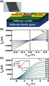
a) Scheme of a field effect transistor device and SEM image of a nanowire connected to two electrodes (source - drain), b), c) curve I = f (Vsd, g) of a NW FET [47]
Fig. 15
Fig. 15
Junction by two crossed nanowires, I-V curves of three types of n-n junction, p-p and p-n [48]
Fig. 16
Fig. 16
Device for pH probes. [53]
Fig. 17
Fig. 17
Detection device based on a silicon nanowire bio-molecular interaction biotin/streptavidin [54]
Fig. 18
Fig. 18
DNA detection process by a probe made of a silicon nanowire modified with a peptide [58]
Fig. 19
Fig. 19
Virus detection by a modified silicon nanowire [59]
Fig. 20
Fig. 20
a) silicon nanowire based solar cells, b) optical characteristic of the nanowire solar cells [64]
Fig. 21
Fig. 21
Left (a-b) Schematic of morphological changes that occur in Si during electrochemical cycling. Right c) XRD patterns of Si NWs before electrochemical cycling (initial),at different potentials during the first charge, and after five cycles. dg), TEM data for Si NWs at different stages of the first charge [77]
Fig. 22
Fig. 22
SEM images of nanowire devices. (a) SEM image at 90° nanowires after growth on TiN and (inset) view of the complete device with the connection pad on the left (scale bar = 75 μm) and (b) in sectional SEM image of a nanowire after the alumina and TiN deposits [89]

References

    1. Cui Y, Zhong Z, Wang D, Wang WU, Lieber CM. Nano Lett. 2003;3:149. doi: 10.1021/nl025875l. - DOI
    1. Cui Y, Lieber CM. Science. 2001;291:851. doi: 10.1126/science.291.5505.851. - DOI - PubMed
    1. Chung J-W, Yu J-Y, Heath JR. Appl. Phys. Lett. 2000;76:2068. doi: 10.1063/1.126257. - DOI
    1. Cui Y, Wei Q, Park H, Lieber CM. Science. 2001;293:1289. doi: 10.1126/science.1062711. - DOI - PubMed
    1. Hahm J, Lieber CM. Nano Lett. 2004;4:51. doi: 10.1021/nl034853b. - DOI

LinkOut - more resources