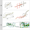
Review
. 2020 Apr 22;9(4):499-511.
doi: 10.1002/open.201900347. eCollection 2020 Apr.

Supramolecular Assembly of Thiophene-Based Oligomers into Nanostructured Fluorescent Conductive and Chiral Microfibers

Affiliations
Review

Supramolecular Assembly of Thiophene-Based Oligomers into Nanostructured Fluorescent Conductive and Chiral Microfibers

Mattia Zangoli et al. ChemistryOpen. .

Abstract

The implementation of nano/microelectronic devices requires efficient strategies for the realization of supramolecular structures with desired function and supported on appropriate substrates. This article illustrates a strategy based on the synthesis of thiophene oligomers having the same "sulfur-overrich" quaterthiophene inner core (non bonding interactional algorithm) and different terminal groups. Nano/microfibers are formed on surfaces having a morphology independent of the nature of the deposition substrate and displaying a wide tuning of properties that make the fibers optoelectronically suitable for application in devices.

Keywords: charge conduction; chirality; nano/microfibers; self-assembly; sulfur-overrich thiophenes.


Conflict of interest statement

The authors declare no conflict of interest.

Figures

Scheme 1
Scheme 1
Molecular structure of the thiophene‐based oligomers reviewed in this article. In red the ‐T4S4‐fragment.
Figure 1
Figure 1
Microfibers deposition by solvent exchange in solution.
Figure 2
Figure 2
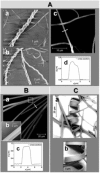
(A) SEM (a and b on SiO2), AFM (c, on glass) and AFM profile (d) of fibers of 1; (B) AFM (a, on glass) and AFM profile (b) of fibers of 2; (C) SEM (a and b on glass) images of fibers of 3. Adapted with permission from reference [11a].
Figure 3
Figure 3
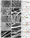
SEM images of fibers of compounds 5 to 9 through the solvent‐exchange method and circular dichroism (CD) plots of two different samples of the fibers of each compound. Adapted with permission from reference [11b].
Figure 4
Figure 4
(A) Topography image (left) and hole transportation measurement (right) of helical fibers of 1 grown on ITO obtained using Tr‐TUNA with a 5 V bias on the tip. (B) The same as panel A for rod‐like fibers of 2. Adapted with permission from reference [11a].
Figure 5
Figure 5
Typical AFM topography (scale bar 1/4 20 mm, z scale 0–250 nm), and corresponding profiles of (a and b) aligned and (c and d) randomly distributed fibers on an interdigitated electrode/SiO2 surface (scale bar 1/4 20 mm, z scales (a) 0–250 nm, (b) 0–500 nm). The inset in (a) shows the AFM topography image of a PDMS stamp (scale bar 1/4 10 mm, z scale 0–250 nm). Here we have shown fibers of 2 (3 and 4 exhibit a similar morphology). Reproduced with permission from reference [23].
Figure 6
Figure 6
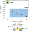
Surface electronic potential measured by KPFM for the fibers of 59 grown on glass and energy diagram for p‐type and n‐type charge carriers. Reproduced with permission from reference [11b].
Figure 7
Figure 7
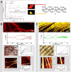
A) Plots of X‐ray analysis of the microcrystalline powders of compound 1. The insets are microscopy fluorescence images of the red and yellow powders. B) From top down: fluorescence image and circular dichroism spectra of two different samples of the red microfibers deposited on glass; AFM and AFM profile of the red microfibers directly grown on a FET device, together with the corresponding electrical transfers in saturation regime. C) The same for the yellow microfibers. Adapted with permission from reference [16].
Figure 8
Figure 8
A), B) Sketches of the proposed unit cells of the fibers of 5 and 8 (axes lengths in nm being obtained from the distances of the main reflections of X‐ray plots and DFT calculated conformations of the dimers of 5, 8. C) NCI (non covalent interaction indicator) isosurface plots for the dimer of compound 8 identifying hydrogen bonding regions (the green regions between the two molecules). For clarity, the isosurfaces were generated only for the regions indicated by the box. Adapted from reference [11b].
Figure 9
Figure 9
A) X‐ray diffraction pattern of the fibers of compounds 14 grown on glass; periodic distances reported in nm; conformation of the inner tetrameric core of the octamers as determined by single crystal X‐ray analysis of compound 2 and model of J‐type stacking. B) A detail of the film from 4 and proposed model for the supramolecular packing. Adapted from reference [11a].
Figure 10
Figure 10
Proposed growth model for the tape‐like and helical crystalline fibers of compounds 19. Reproduced with permission from reference [11b].

References

    1. None
    1. Xu K., Xie S., Instrum. Sci. Technol. 2019. https://doi.org/10.1080/10739149.2019.1660182;
    1. Chochos C. L., Spanos M., Katsouras A., Tatsi E., Drakopoulou S., Gregoriou V. G., Avgeropoulos A., Prog. Polym. Sci. 2019, 91, 51–79;
    1. Ouchi H., Lin X., Yagai S., Chem. Lett. 2019, 48, 1009–1018;
    1. V. Vohra, T. Anzai. J. Nanomater 2017, vol. 2017, Article ID 3624750, 18 pages. https://doi.org/10.1155/2017/3624750;

Publication types

LinkOut - more resources