. 2020 Apr 29;11(1):2069.
doi: 10.1038/s41467-020-15933-2.

In-situ resonant band engineering of solution-processed semiconductors generates high performance n-type thermoelectric nano-inks

Affiliations

In-situ resonant band engineering of solution-processed semiconductors generates high performance n-type thermoelectric nano-inks

Ayaskanta Sahu et al. Nat Commun. .

Abstract

Thermoelectric devices possess enormous potential to reshape the global energy landscape by converting waste heat into electricity, yet their commercial implementation has been limited by their high cost to output power ratio. No single "champion" thermoelectric material exists due to a broad range of material-dependent thermal and electrical property optimization challenges. While the advent of nanostructuring provided a general design paradigm for reducing material thermal conductivities, there exists no analogous strategy for homogeneous, precise doping of materials. Here, we demonstrate a nanoscale interface-engineering approach that harnesses the large chemically accessible surface areas of nanomaterials to yield massive, finely-controlled, and stable changes in the Seebeck coefficient, switching a poor nonconventional p-type thermoelectric material, tellurium, into a robust n-type material exhibiting stable properties over months of testing. These remodeled, n-type nanowires display extremely high power factors (~500 µW m-1K-2) that are orders of magnitude higher than their bulk p-type counterparts.


Conflict of interest statement

A.S., B.R., M.L., F.Y., J.D.F., N.E.C., R.A.S., and J.J.U. are listed as inventors on a patent filed by the University of California, Berkeley in September 2016, entitled “Surface Doping of Nanostructures” for the surface doping procedure described in Fig. 1.

Figures

Fig. 1
Fig. 1. Resonant band engineering by interfacial resurfacing.
a, b Schematic of the doping process (not to scale) showing the evolution of the density of states and the change in Fermi level with removal of the polymer (polyvinylpyrrolidone, PVP) and attachment of the sulfur (S2−) atoms. CB and VB stand for conduction band and valence band, respectively. At low sulfur concentration, isolated states originate close to the CB of tellurium which transform to a prominent sulfur-generated dopant band at high concentrations. ce Transmission electron micrographs of undoped, intermediate- and heavily doped 80-nm diameter tellurium (Te) nanowires (NWs), respectively. The insets show high resolution images with both the inorganic component and the polymer layer. While one can observe a thick polymer layer in c, the doped sample in d shows a thinner layer and the one in e shows no evidence of any polymer.
Fig. 2
Fig. 2. Structural characterization of dopant location.
a High-angle annular dark-field scanning transmission electron microscopy (HAADF-STEM) and b, c energy-dispersive X-ray (EDX) maps of sulfur and tellurium, respectively, in a sulfur-doped tellurium nanowire showing the presence of minute amounts of sulfur in the sample d line scans demonstrating that sulfur atoms are primarily concentrated on the surface of the nanowire.
Fig. 3
Fig. 3. Charge transfer and evolution of a resonant dopant band with sulfur doping.
a Illustration of the atomistic structure and (010) surface, of the hexagonal tellurium nanowire using density functional theory calculations. The supercell configuration and the charge-transfer effect for b physical adsorption and c chemical adsorption of equal amount of sulfur adatoms on tellurium along (010) surface. The blue isosurface represents injection of electrons, and red for stripping or withdrawal of electrons. For clarity, the iso-charge contours are only shown in the right halves of b and c. Plane-integrated charge transfer along the surface normal direction is shown for both cases and is plotted with the same scale, so that they are quantitatively comparable. d, e Calculatedsurface density of states using density functional theory (DFT) for tellurium (p-type) and sulfur-doped tellurium (n-type) with CB and VB referring to the conduction and valence bands of bulk tellurium, respectively. The dotted black line denotes the edge of the CB. A new dopant band (shaded ellipse) emerges close to the conduction band edge for the sulfur-doped tellurium.
Fig. 4
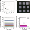
Fig. 4. Tuning Seebeck coefficients with controlled doping.
a Seebeck coefficient from a series of doped Te NW samples versus the amount of S2− added to the exchange solution, normalized to the total number of Te atoms present on the surface of the NW. b Representative set of smooth drop-cast films used for the measurements. c Short-term stability tests from a series of Te NW samples with varying doping concentrations. d Long-term stability tests for as-synthesized p-type Te NWs capped with polyvinylpyrrolidone (black) and multiple batches of fully surface exchanged Te NWs with S2− (colors). The data in green is from a sample stored in ambient for nearly 7 months and the data in red is from a device stored in the glove box for 23 months.
Fig. 5
Fig. 5. Fermi level shifts with doping.
a Schematic cross-section (not to scale) of ion-gel-gated thin-film transistors used to characterize the electrical properties of the doped NWs. The length and width of the channel were 100 μm and 2 mm, respectively. Red and blue circles represent positive and negative ions, respectively. b Energy level diagram depicting the relationship between the location of the Fermi energy (EF), band-edges, doping concentration, and corresponding nature of charge carriers. CB and VB refer to the conduction band and the valence band of Te, respectively. Transfer characteristics for the c undoped Te-PVP NW sample (with VD = 0.1 V) showing p-type transport, d intermediate-doped Te NWs (~1.5% atomic concentration of sulfur, with VD = −0.3 V) showing ambipolar transport. e Heavily doped Te NWs (~2.4% atomic concentration of sulfur, with VD = −1.5 V) showing n-type transport. Black and red curves plot the characteristics on logarithm and linear scales respectively.
Fig. 6
Fig. 6. Thermoelectric transport properties in surface re-engineered tellurium nanowires.
a Temperature-dependent conductivity (σ) measurements (from 90 to 225 K) on thin films of undoped p-type (Te-PVP, blue spheres) and sulfur-doped n-type (Te–S2−, red spheres) tellurium nanowires normalized to the respective conductivity values at 90 K (σ90K). While the undoped nanowire films show activated (semiconductor-like) transport with conductivities increasing with increasing temperature, the doped nanowire films demonstrate band-like transport with decreasing values of conductivities with increasing temperature. b Proposed doping scheme wherein sulfur dopes tellurium n-type and most of the electrons are located in the dopant band with the Fermi level inside the band (similar to a metal) at low temperatures (below 225 K), and hence the band-like transport behavior. Above 225 K, the electrons gain sufficient thermal energy to get promoted to the conduction band. c Temperature-dependent conductivity measurements for the n-type (Te–S2−) samples wherein above 225 K the conductivity increases sharply with increasing temperature. Temperature-dependent d electrical conductivity, e Seebeck coefficient, and f power factor of the n-type Te nanowire film demonstrating extremely high monotonously increasing power factors with increasing temperature.
Fig. 7
Fig. 7. Thermoelectric generator demonstrations for in-plane devices.
a A flexible module prepared from solution-processable Te NW inks in an unconventional thin-film leg-geometry. b Module n- and p-type legs drop-cast onto Kapton substrate to make the array shown in a. c Infrared image depicting a temperature gradient of 15 °C established across the thin-film module. d Total module open-circuit voltage (VOC) generated as a result of the Seebeck effect as a function of the number of n- and p-type legs connected in series in the module depicted in ac. Additive nature of the VOC confirms the proper working of the module.

References

    1. Bell LE. Cooling, heating, generating power, and recovering waste heat with thermoelectric systems. Science. 2008;321:1457–1461. doi: 10.1126/science.1158899. - DOI - PubMed
    1. Snyder GJ, Toberer ES. Complex thermoelectric materials. Nat. Mater. 2008;7:105–114. doi: 10.1038/nmat2090. - DOI - PubMed
    1. Yau, C.-W., Kwok, T. T.-O., Lei, C.-U., Kwok, Y.-K. Energy harvesting in internet of things. in Internet of Everything: Algorithms, Methodologies, Technologies and Perspectives (eds Di Martino, B., Li, K.-C., Yang, L. T. & Esposito, A.) (Springer, Singapore, 2018).
    1. Bahk J-H, Fang H, Yazawa K, Shakouri A. Flexible thermoelectric materials and device optimization for wearable energy harvesting. J. Mater. Chem. C. 2015;3:10362–10374. doi: 10.1039/C5TC01644D. - DOI
    1. Hannan MA, Mutashar S, Samad SA, Hussain A. Energy harvesting for the implantable biomedical devices: issues and challenges. Biomed. Eng. OnLine. 2014;13:79. doi: 10.1186/1475-925X-13-79. - DOI - PMC - PubMed