. 2020 May 7;11(1):2245.
doi: 10.1038/s41467-020-16105-y.

Perovskite neural trees

Affiliations

Perovskite neural trees

Hai-Tian Zhang et al. Nat Commun. .

Abstract

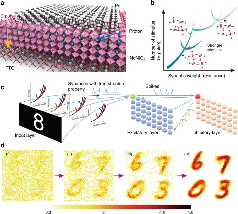
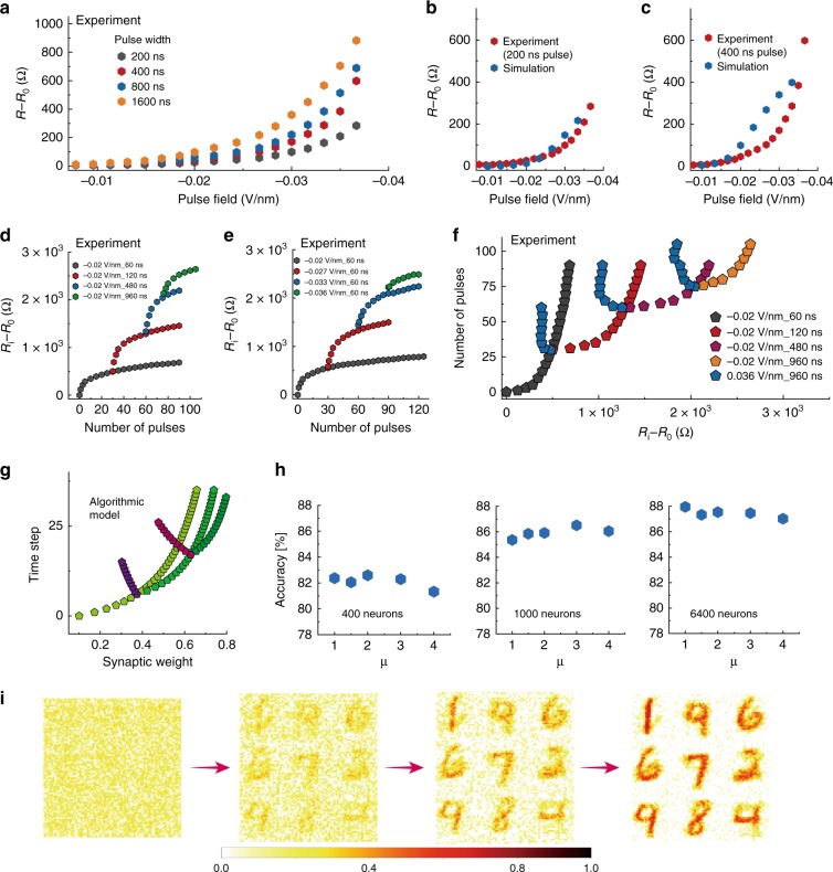
Trees are used by animals, humans and machines to classify information and make decisions. Natural tree structures displayed by synapses of the brain involves potentiation and depression capable of branching and is essential for survival and learning. Demonstration of such features in synthetic matter is challenging due to the need to host a complex energy landscape capable of learning, memory and electrical interrogation. We report experimental realization of tree-like conductance states at room temperature in strongly correlated perovskite nickelates by modulating proton distribution under high speed electric pulses. This demonstration represents physical realization of ultrametric trees, a concept from number theory applied to the study of spin glasses in physics that inspired early neural network theory dating almost forty years ago. We apply the tree-like memory features in spiking neural networks to demonstrate high fidelity object recognition, and in future can open new directions for neuromorphic computing and artificial intelligence.


Conflict of interest statement

The authors declare no competing interests.

Figures

Fig. 1
Fig. 1. Perovskite neural trees and their use in neuromorphic learning.
a Schematic figure of the perovskite nickelate NdNiO3 device with Pd as top electrode and fluorine-doped tin oxide (FTO) as bottom electrode. The top electrode serves also to catalytically dope hydrogen into the near-surface region of the perovskite. Applying electric field pulses can move the protons in the lattice which also changes the local Ni valence state and electron-electron correlation, thus modulating the device resistance in a systematic manner. b Schematic of the tree structure showing synaptic strength (resistance) as function of number of stimulus (electric pulses). The electrical resistance of the perovskite devices can be modulated with consecutive electric pulses. The snapshots schematically show the movement of protons in the lattice, which leads to different resistivity values. c Architecture of spiking neural network for handwritten digit recognition. Each input image pixel is assigned to one input neuron. Input layer generates Poisson’s distributed spike train depending on the pixel intensity values, which potentiates the membrane potential (Vmem) of excitatory layer neuron. These spikes are propagated from input to excitatory layer through synapses which learns using spike time dependent plasticity (STDP) learning rule. Once membrane potential reaches a threshold (Vthresh), the neuron generates a spike and synapse weights are updated. The tree structure graph represents how synaptic weight changes with input strength. Different curves correspond to different constant inputs. d Evolution of digit learning using the tree-like synapses. Step (I) shows the synapse weights at initial stages of learning, (II) and (III) show weights after learning from 10,000 and 30,000 training images, and (IV) is the final learned weights after training on 60,000 images.
Fig. 2
Fig. 2. Experimental data of electrical behavior and simulation in neural networks.
a Change in electrical resistance of the nickelate device after voltage pulses were applied with different pulse field and pulse width. The change in resistance is proportional to both the pulse field and pulse width. b, c Modeling and experimental results of the change in resistance after application of various voltage pulses, b 200 ns pulse, and c 400 ns pulse widths. d, e The electrical response of the nickelate device to consecutive electrical pulses. The different colors in (d) represent different pulse widths, while the different colors in (e) represent different pulse field. The structure was generated following the method shown in Supplementary Fig. 6. f By applying consecutive positive or negative pulses, tree structure comprising different resistance states can be generated, with characteristics similar to synaptic behavior in the central nervous system,–. The same colored data points correspond to a fixed input that is applied to the device. g Algorithmic weight change as a function of learning time steps. The synaptic weight update mechanism has a tree structure that is inherently possessed by the nickelate devices (for μ = 3). h Object recognition testing accuracy of a spiking neural network on Modified National Institute of Standards and Technology database (MNIST) dataset when trained with different μ values on 400, 1000, and 6400 excitatory neurons. Testing accuracy change of about ±0.5% is observed, which does not significantly hamper the network’s digit recognition performance, hence the network is sufficiently immune to variations in μ. i Weight evolution of nine neurons when the spiking neural network is trained using spike time dependent plasticity (STDP) learning rule. The learning evolves such that the weights associated with each neuron approximates one of the variations of the digit learned by that neuron since each neuron in excitatory layer is connected to all neurons of the input layer.
Fig. 3
Fig. 3. Microscopic mechanism leading to the tree-like synaptic memory.
a Scheme of the nanoprobe X-ray absorption imaging experiment. The incoming X-ray beam is focused by the Fresnel zone plate, and diffraction orders are filtered out by the order-sorting aperture (OSA). The fluorescence signal at the K-edge of Ni from the 30-nm spot illuminated by the X-rays is recorded by the detector positioned perpendicular to the beam. A scanning electron microscope (SEM) image of the nickelate device is shown at the bottom. The red rectangle shows the scanned area of the X-ray absorption imaging. b Changes in the XAS spectrum at Ni K-edge as the probe is rastered across the device channel. The spectra were measured at different positions between the electrodes and averaged along the electrode edge, starting from the Pd electrode (the lowest spectrum) to the Au electrode (the upper spectrum). The distance between two successive spectra is Δy  =  200  nm. The dashed line is shown for better visualization of the peak shift. From the Au electrode to the Pd electrode, the Ni K-edge peak shifts to lower energy, indicating the change in Ni valence and proton doping near the Pd electrode. c The fitted energy value of the Ni K-edge peak plotted as function of sample position. The fitting error is ~0.15  eV which was calculated by using different fitting procedures and evaluating the distribution of the obtained values of Epeak. d, e, f Changes in Ni K-edge fluorescence intensity of the hydrogenated nickelate device after electrical stimuli. The color corresponds to the intensity of the normalized fluorescence signal at the fixed energy of E  =  8345  eV (where the slope of the XAS curve is highest and thus most sensitive to the energy shift) and therefore characterizes the hydrogen doping of the channel. Dashed lines denote the positions of the Au and Pd electrodes. The map of the initial sample is shown in panel (d), the map after applying several 2 mV pulses of 5 -s duration time is shown in (e), and after several 1  V pulses of 100- ns duration in (f). g Atomic-scale pathway, and the associated energy barriers for various applied e-fields for surface proton doping into the nickelate lattice. The potential energy along the most preferred migration pathway (as obtained from nudged-elastic band (NEB) DFT calculations) is shown on the left, while selected configurations along this pathway labeled I1–I3 are depicted on the right. A barrier of 0.9 eV was obtained for this depicted proton intercalation pathway with no field. Electric fields reduce the barrier—a 50% reduction in barrier is seen for an applied e-field of 0.055  V/nm. Two different pathways for proton diffusion in the bulk are shown. Panel (h) represents a lower (preferred) pathway, whereas (i) represents a high energy barrier for bulk diffusion in the presence of the e-field. For all the depicted configurations, only two NiO6 octahedra are shown for clarity; the Ni, O, and H ions are represented by gray, red, and green spheres, respectively.

References

    1. Burr GW, et al. Neuromorphic computing using non-volatile memory. Adv. Phys. X. 2017;2:89–124.
    1. Wang Y, et al. Mott-transition-based RRAM. Mater. Today. 2019;28:63–80. doi: 10.1016/j.mattod.2019.06.006. - DOI
    1. Guo Y, Wu H, Gao B, Qian H. Unsupervised learning on resistive memory array based spiking neural networks. Front. Neurosci. 2019;13:812. doi: 10.3389/fnins.2019.00812. - DOI - PMC - PubMed
    1. Zhou Y, Ramanathan S. Mott memory and neuromorphic devices. Proc. IEEE. 2015;103:1289–1310. doi: 10.1109/JPROC.2015.2431914. - DOI
    1. Andrews JL, Santos DA, Meyyappan M, Williams RS, Banerjee S. Building brain-inspired logic circuits from dynamically switchable transition-metal oxides. Trends Chem. 2019;1:711–726. doi: 10.1016/j.trechm.2019.07.005. - DOI

Publication types