. 2020 May 11:9:83.
doi: 10.1038/s41377-020-0268-1. eCollection 2020.

Micro-light-emitting diodes with quantum dots in display technology

Affiliations

Micro-light-emitting diodes with quantum dots in display technology

Zhaojun Liu et al. Light Sci Appl. .

Abstract

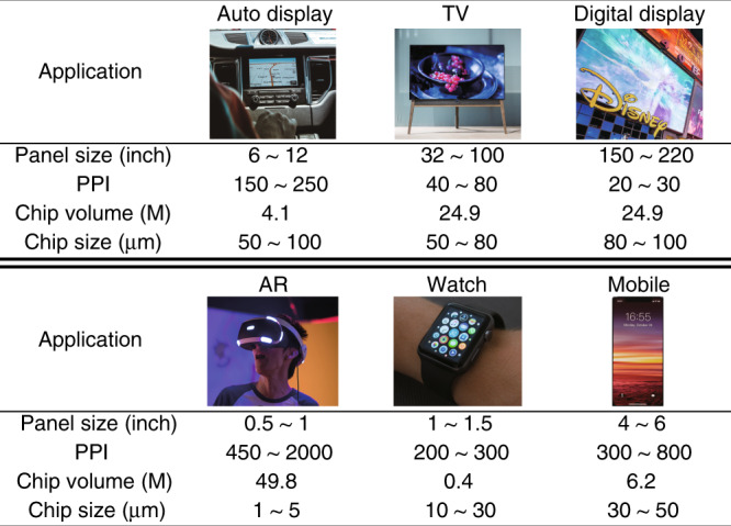
Micro-light-emitting diodes (μ-LEDs) are regarded as the cornerstone of next-generation display technology to meet the personalised demands of advanced applications, such as mobile phones, wearable watches, virtual/augmented reality, micro-projectors and ultrahigh-definition TVs. However, as the LED chip size shrinks to below 20 μm, conventional phosphor colour conversion cannot present sufficient luminance and yield to support high-resolution displays due to the low absorption cross-section. The emergence of quantum dot (QD) materials is expected to fill this gap due to their remarkable photoluminescence, narrow bandwidth emission, colour tuneability, high quantum yield and nanoscale size, providing a powerful full-colour solution for μ-LED displays. Here, we comprehensively review the latest progress concerning the implementation of μ-LEDs and QDs in display technology, including μ-LED design and fabrication, large-scale μ-LED transfer and QD full-colour strategy. Outlooks on QD stability, patterning and deposition and challenges of μ-LED displays are also provided. Finally, we discuss the advanced applications of QD-based μ-LED displays, showing the bright future of this technology.

Keywords: Inorganic LEDs; Quantum dots.


Conflict of interest statement

Conflict of interestThe authors declare that they have no conflict of interest.

Figures

Fig. 1
Fig. 1
Pixels per inch roadmap of µ-LED displays from 2007 to 2019
Fig. 2
Fig. 2
Positional relation between leakage spots and defect states. The emission microscopy measurement shows a strong relation between a leakage spots and b etch pits (~1 μm size), confirming the importance of defect control during epitaxy. The dashed line and circles indicate the mesa edge and leakage spots, respectively. Reproduced from ref. with permission from AIP Publishing
Fig. 3
Fig. 3
Size reduction effect on μ-LED performance. EQE of GaN μ-LED as a function of LED size. Data compiled from ref.
Fig. 4
Fig. 4
Sidewall passivation effect in μ-LEDs. a Schematic of the μ-LED structure with ALD deposited SiO2 for sidewall passivation. b Electroluminescence images of the μ-LEDs (sizes from 10 μm to 100 μm) before and after sidewall passivation. c The EQE distribution of different device sizes with and without KOH treatment and ALD sidewall passivation. Reproduced from a, b ref. with permission from OSA and c ref. with permission from Copyright (2019) The Japan Society of Applied Physics
Fig. 5
Fig. 5
Strain relaxation in small LEDs observed by Kelvin probe force microscopy. Topographic and CPD distribution of μ-LEDs with a 10-μm and b 40-μm diameters. The central bright region is the LED mesa. Reproduced from ref. with permission from OSA
Fig. 6
Fig. 6
μ-LED mass transfer techniques. Schematics of a elastomer stamping, b electrostatic/electromagnetic transfer, c laser-assisted transfer and d fluid self-assembly. Reproduced from a ref. with permission from Springer Nature, c ref. with permission from MDPI and d ref. with permission from IOP Publishing
Fig. 7
Fig. 7
μ-LED monolithic integration techniques. Schematics of a metal wiring, b flip chip bonding, c microtube bonding and d adhesive bonding. Reproduced from a ref. with permission from Elsevier, b ref. with permission from AIP Publishing, c ref. with permission from John Wiley and Sons and d ref. with permission from RSC Publishing
Fig. 8
Fig. 8
Process flow of the full-colour µ-LED display with photoresist mould design. a The structure of the µ-LED arrays. b Aligning the mould to the UV µ-LED array. ce Consequently jetting the RGB QDs inside the mould window to form the full-colour pixels. Reproduced from ref. with permission from Chinese Laser Press
Fig. 9
Fig. 9
Förster resonant energy transfer nanohole design in LEDs. a Schematic representation, b cross-sectional, and c top scanning electron microscope images of a photonic nanohole LED hybridised with QD colour converters. d Time-resolved photoluminescence decays of LED with pure MQW (black line) and MQW-QD contact (red line) structures. Reproduced with minor editing from ref. the Optical Society under the terms of the Creative Commons Attribution 4.0 License
Fig. 10
Fig. 10
Full-colour QD-NR μ-LED display design and performance. a Epitaxial wafer. b Three subpixels of a green μ-LED, a blue NR μ-LED, and a red QD-NR μ-LED. c Deposition of transparent conducting oxide film and p-n electrodes. d Covering DBR filter. e Full-colour QD-NR μ-LED display. f Cross-sectional view of a single RGB pixel. g EL spectra of a QD-NR μ-LED display. h Colour gamut of a QD-NR μ-LED display, NTSC, and Rec. 2020. Reproduced from ref. with permission from Chinese Laser Press
Fig. 11
Fig. 11
Perovskite QDs for wide colour gamut conversion. a Colloidal CsPbX3 (X = Cl, Br, I) QD solutions in toluene under a UV lamp and b their representative PL spectra. c CIE chromaticity coordinates (dark points) from the emissions of CsPbX3 QDs compared with those of commercialised LCD TVs (dashed white line), reaching 140% of the NTSC colour standard (solid white line). Reproduced from ref. with permission from ACS Publications
Fig. 12
Fig. 12
Strategies for improving the stability of perovskite QDs. a A-site or B-site doping. b Surface engineering. c Encapsulation with a polymer or oxide matrix. d More efficient device packaging (i.e., remote-type design can enhance the stability of QDs compared with the prototype structure). Reproduced from a ref. with permission from RSC Publishing, b ref. with permission from AAAS, c ref. with permission from John Wiley and Sons, and d ref. with permission from RSC Publishing
Fig. 13
Fig. 13
Requirements for µ-LEDs in typical applications. Reproduced from ref. with permission from MDPI

References

    1. Jin SX, et al. GaN microdisk light emitting diodes. Appl. Phys. Lett. 2000;76:631–633. doi: 10.1063/1.125841. - DOI
    1. Day, J. et al. Full-scale self-emissive blue and green microdisplays based on GaN micro-LED arrays. In Proc. SPIE 8268, Quantum Sensing and Nanophotonic Devices IX (SPIE, San Francisco, CA, USA, 2012).
    1. Tian PF, et al. Fabrication, characterization and applications of flexible vertical InGaN micro-light emitting diode arrays. Opt. Express. 2016;24:699–707. doi: 10.1364/OE.24.000699. - DOI - PubMed
    1. Liu ZJ, et al. Monolithic LED microdisplay on active matrix substrate using flip-chip technology. IEEE J. Sel. Top. Quantum Electron. 2009;15:1298–1302. doi: 10.1109/JSTQE.2009.2015675. - DOI
    1. Liu, Z. J. et al. Fully multi-functional GaN-based micro-LEDs for 2500 PPI micro-displays, temperature sensing, light energy harvesting, and light detection. In Proc. 2018 IEEE International Electron Devices Meeting pp. 38.1.1–38.1.4. (IEEE, San Francisco, CA, USA, 2018).