. 2020 May 15;11(1):2407.
doi: 10.1038/s41467-020-16269-7.

Integrated nano-optomechanical displacement sensor with ultrawide optical bandwidth

Affiliations

Integrated nano-optomechanical displacement sensor with ultrawide optical bandwidth

Tianran Liu et al. Nat Commun. .

Erratum in

Abstract

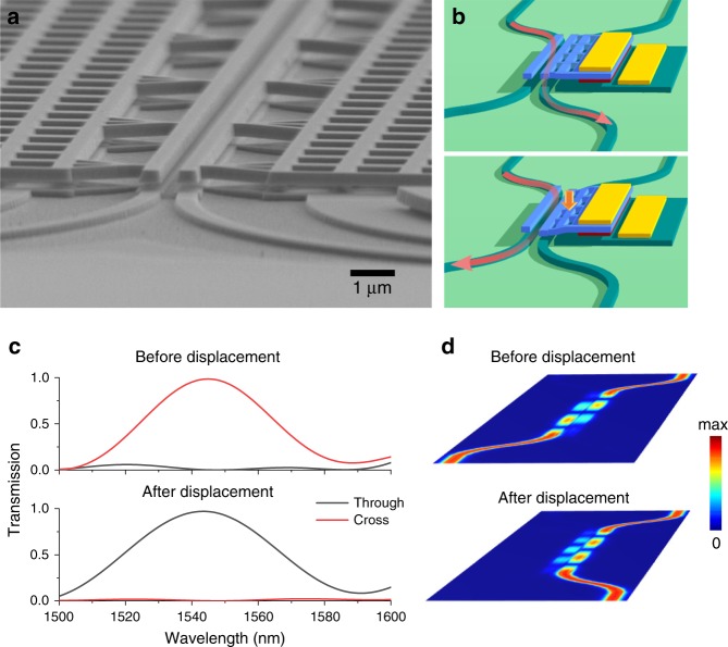
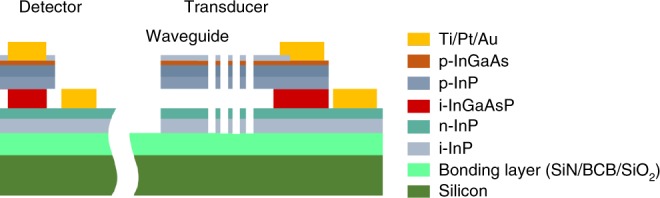
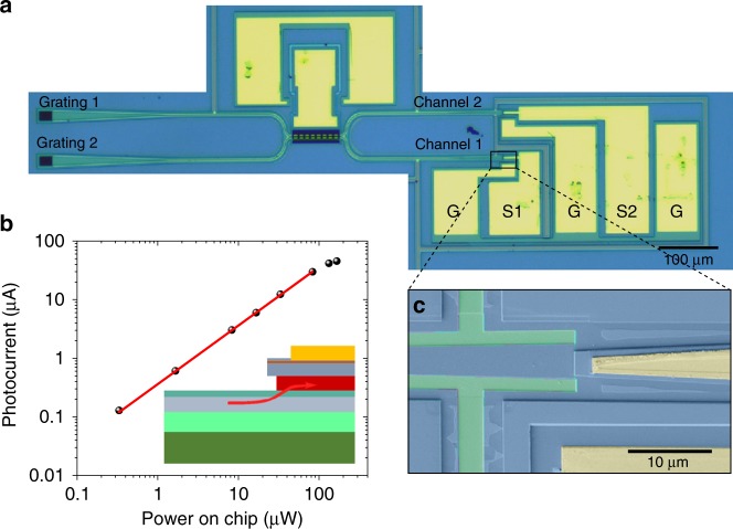
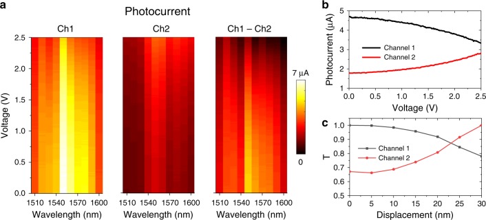
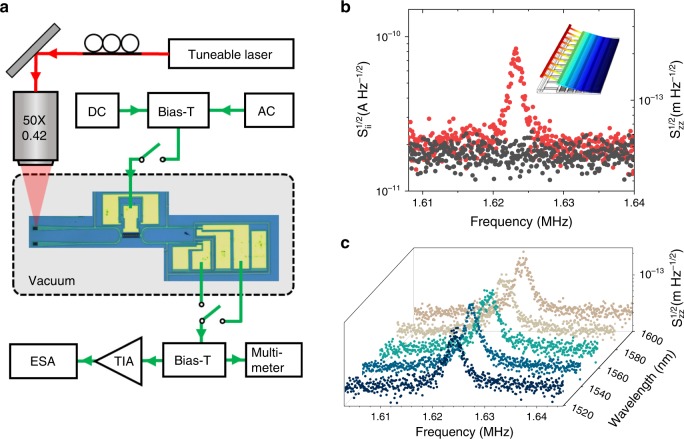
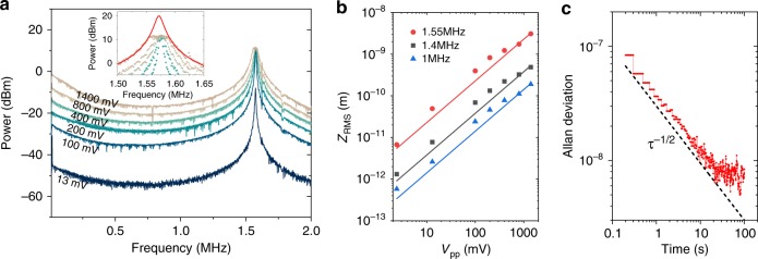
Optical read-out of motion is widely used in sensing applications. Recent developments in micro- and nano-optomechanical systems have given rise to on-chip mechanical sensing platforms, potentially leading to compact and integrated optical motion sensors. However, these systems typically exploit narrow spectral resonances and therefore require tuneable lasers with narrow linewidth and low spectral noise, which makes the integration of the read-out extremely challenging. Here, we report a step towards the practical application of nanomechanical sensors, by presenting a sensor with ultrawide (∼80 nm) optical bandwidth. It is based on a nanomechanical, three-dimensional directional coupler with integrated dual-channel waveguide photodiodes, and displays small displacement imprecision of only 45 fm/Hz1/2 as well as large dynamic range (>30 nm). The broad optical bandwidth releases the need for a tuneable laser and the on-chip photocurrent read-out replaces the external detector, opening the way to fully-integrated nanomechanical sensors.


Conflict of interest statement

The authors declare no competing interests.

Figures

Fig. 1
Fig. 1. Displacement transducing by nanomechanical directional coupler.
a Scanning electron microscope (SEM) image of the nanomechanical directional coupler used as a transducer. b Schematic illustration of light passing through the direction coupler before (up) and after (down) actuation. c Simulated transmission and d simulated electric field distribution (|E|) before and after displacement (55 nm) of an ideal device described in ref. .
Fig. 2
Fig. 2. Schematic cross-section of the layer stack of the device.
The detector (left) and the transducer/actuator part (right).
Fig. 3
Fig. 3. Integrated sensor and response of the photodiode.
a Optical microscope image of the integrated displacement sensor. G stands for ground, S1 and S2 stand for signal of channel 1 and channel 2. b Photocurrent measured on a waveguide photodiode connected directly with a grating coupler at 1540 nm as a function of power on chip. Linear fit of the photocurrent with power under 100 µW is indicated by red line. Inset: Schematic of the integrated photodiode. Red arrow marks the direction of incoming light. c SEM image of the integrated photodiode in false colors.
Fig. 4
Fig. 4. Response of the senor under a static actuation.
a Photocurrent of the two detectors and their difference, as a function of reverse bias voltage on the actuator, for an on-chip laser power of 0.3 mW. b Measured photocurrent at 1540 nm as a function of bias voltage. c Simulated transmittance at 1540 nm as a function of the displacement of the suspended waveguide.
Fig. 5
Fig. 5. Experimental set-up and the measurement of the thermal noise.
a Schematics of the thermal noise measurement setup. b Photocurrent (left axis) and displacement (right axis) spectral density, measured by the ESA with (red circles) and without (black circles) laser (λ = 1540 nm, on-chip power 0.3 mW, actuator bias voltage 1.5 V), showing a peak corresponding to the Brownian motion of the fundamental mechanical mode. Inset: Calculated mode shape of fundamental mechanical mode. c Brownian motion measured at different wavelengths.
Fig. 6
Fig. 6. Response of the sensor driven by an oscillating voltage.
a Driven-response spectra for various driving amplitude measured with a 50 Hz resolution bandwidth. A −1 V DC bias is applied for Vpp from 13 mV to 800 mV. For Vpp = 1.4 V a −1.4 V DC bias is used. Inset: Zoom-in of the spectra around at the resonance, with a Lorentzian fit of the 1.4 V modulation data. Laser wavelength is 1540 nm and on-chip power 0.3 mW. b Root mean square displacement of cantilever as a function of peak-to-peak voltage at 1.55 MHz, 1.4 MHz and 1 MHz. Dots are measurement data and solid lines are linear fits. c Allan deviation as a function of integration time. The τ−1/2 slope is indicated with dashed line, where τ is the integration time.

References

    1. Metcalfe M. Applications of cavity optomechanics. Appl. Phys. Rev. 2014;1:031105. doi: 10.1063/1.4896029. - DOI
    1. Hu Y, et al. Optomechanical sensing with on-chip microcavities. Front. Phys. 2013;8:475–490. doi: 10.1007/s11467-013-0384-y. - DOI
    1. Roy, S. K. et al. Improving mechanical sensor performance through larger damping. Science360, eaar5220 (2018). - PubMed
    1. Gavartin E, Verlot P, Kippenberg TJ. A hybrid on-chip optomechanical transducer for ultrasensitive force measurements. Nat. Nanotechnol. 2012;7:509–514. doi: 10.1038/nnano.2012.97. - DOI - PubMed
    1. Wilson DJ, et al. Measurement-based control of a mechanical oscillator at its thermal decoherence rate. Nature. 2015;524:325. doi: 10.1038/nature14672. - DOI - PubMed