. 2020 May 15;11(1):2413.
doi: 10.1038/s41467-020-16190-z.

Modular nonlinear hybrid plasmonic circuit

Affiliations

Modular nonlinear hybrid plasmonic circuit

Alessandro Tuniz et al. Nat Commun. .

Abstract

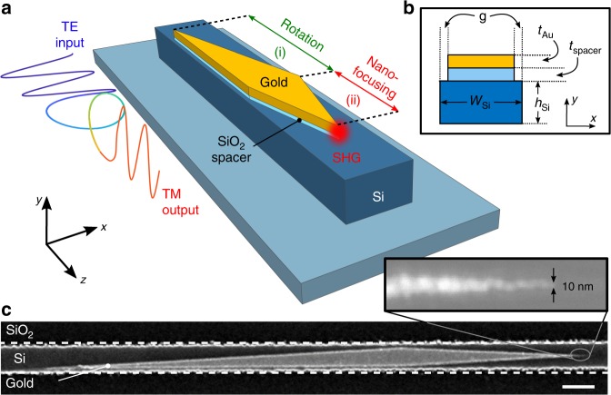
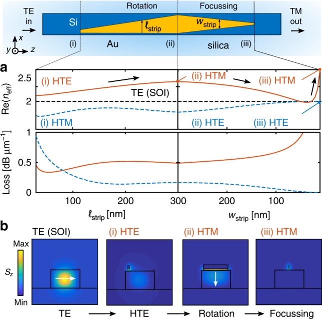
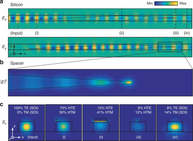
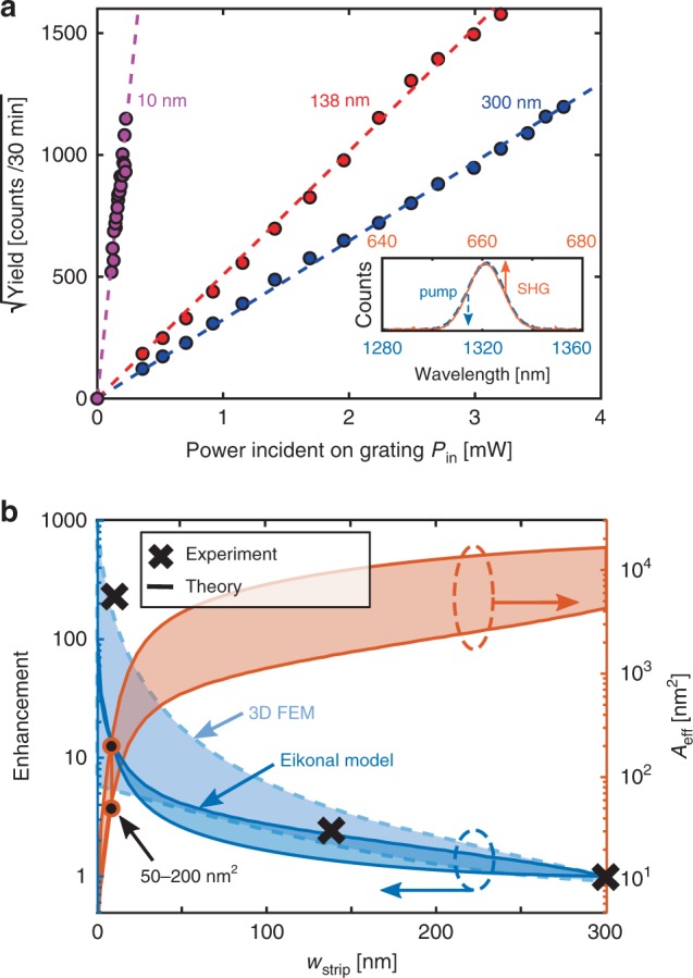
Photonic integrated circuits (PICs) are revolutionizing nanotechnology, with far-reaching applications in telecommunications, molecular sensing, and quantum information. PIC designs rely on mature nanofabrication processes and readily available and optimised photonic components (gratings, splitters, couplers). Hybrid plasmonic elements can enhance PIC functionality (e.g., wavelength-scale polarization rotation, nanoscale optical volumes, and enhanced nonlinearities), but most PIC-compatible designs use single plasmonic elements, with more complex circuits typically requiring ab initio designs. Here we demonstrate a modular approach to post-processes off-the-shelf silicon-on-insulator (SOI) waveguides into hybrid plasmonic integrated circuits. These consist of a plasmonic rotator and a nanofocusser, which generate the second harmonic frequency of the incoming light. We characterize each component's performance on the SOI waveguide, experimentally demonstrating intensity enhancements of more than 200 in an inferred mode area of 100 nm2, at a pump wavelength of 1320 nm. This modular approach to plasmonic circuitry makes the applications of this technology more practical.


Conflict of interest statement

The authors declare no competing interests.

Figures

Fig. 1
Fig. 1. Schematic and scanning electron micrograph of silicon-on-insulator hybrid plasmonic circuit.
a An industry-standard TE ridge waveguide is followed by two in-series plasmonic circuit modules: (i) efficient TE-photonic to TM-plasmonic rotator and (ii) nano-focusing tip. b Geometric parameters at the rotator-focuser boundary. c Scanning electron micrograph (SEM) of a fabricated device. Scale bar: 400 nm. Here, wSi = 350 nm; hSi = 220 nm; g = 25 nm; tspacer = 20 nm; tAu = 50 nm Inset: high-resolution nanotip detail, revealing 10 nm apex sharpness.
Fig. 2
Fig. 2. Two-dimensional calculations of relevant optical modes.
a Calculated effective index Re(neff) and loss for relevant modes (λ = 1.32 μm). Red line: a TE mode at input (TE SOI) (i) couples to a hybrid TE (HTE) mode, (ii) evolving to a rotated hybrid TM (HTM) mode, and (iii) transitions to a nano-focused HTM plasmonic mode. The dashed blue line shows the HTM-to-HTE evolution. b Corresponding mode profiles as labeled. White arrows represent the dominant electric field direction. The color represents the z-component of the time-averaged Poynting vector Sz. Window size: 0.8 × 0.8 μm2. See Fig. 1 caption for relevant parameters.
Fig. 3
Fig. 3. Three-dimensional finite element simulations showing device performance.
a Electric field components in the xy plane (a) in the middle of the silicon waveguide, showing polarization rotation (vanishing Ex and emerging Ey). Window size: 7 × 1 μm2. b Field intensity ∣E2 in the middle of the spacer, showing nano-concentration of energy. Window size: 1.5 × 0.2 μm2. c Time-averaged Poynting vector Sz at each of the locations (i)–(iv) and input as labeled in (a). Inset: relative contribution (in %) for each mode shown in Fig. 2.
Fig. 4
Fig. 4. Measurements of polarization rotation.
a Microscope image of a 20 μm WG with an HPIC (SEM inset). Light is coupled to the waveguide using a TE grating at input. b Measured light from the output TE grating and the tip (dashed line in (a)). c Placing a polarizer between scattered light and camera confirms that light from the tip is TM polarized, while light from the grating is TE polarized. White arrows in (c) show polarizer orientation. d Measured light scattered by the output grating with and without the HPIC, resulting in 13% relative transmittance. Colorscale in (b), (c), and (d) represents the number of photon counts measured by the InGaAs camera, divided by the maximum number of counts measured in (b) and (d), respectively.
Fig. 5
Fig. 5. Measurements of pump- and second-harmonic light scattered by the gold nanotips.
a SOI-HPIC scanning electron micrographs, with tip width of 300 nm (blue), 138 nm (red), and 10 nm (magenta). Measured scattering from the SOI-HPIC b in the NIR c and visible. Images in (b) and (c) are respectively captured under the same conditions, unless otherwise indicated. Pin is the average power incident onto the input grating for the three captured images in (c). The color bar represents the number of counts measured in (b) and (c), divided by the maximum number of counts in (b) and (c), respectively.
Fig. 6
Fig. 6. Experimental demonstration of nanoscale intensity enhancement in the HPIC.
a Circles: square root of the measured yield for each sample (color coding as in Fig. 5). Dashed lines: linear fits confirming quadratic dependence on incident power (ISHG1/2Pin). Inset: spectra of the pump (blue), and of the SHG from the tip (orange). b Calculated enhancement (left axis, solid line) and effective area (right axis, dashed line) as a function of strip width for a focuser length of 3 μm, relative to the largest wstrip = 300 nm, following. Light- and dark-blue shadow encompass the enhancement values predicted by full 3D simulations and the Eikonal model respectively, see Supplementary Fig. 5b. Black crosses show the experimentally measured relative increase in intensity, obtained from the square of the slopes in (a)—error bars from confidence intervals of the straight line fits in (a) are smaller than symbol size. Black circles: calculated effective area range of 50– 200 nm2 for wstrip = 10 nm.

References

    1. Chrostowski, L. & Hochberg, M. Silicon Photonics Design: From Devices to Systems (Cambridge University Press, 2015).
    1. Dong P, et al. Monolithic silicon photonic integrated circuits for compact 100+ Gb/s coherent optical receivers and transmitters. IEEE J. Sel. Top. Quantum Electron. 2014;20:150–157. doi: 10.1109/JSTQE.2013.2295181. - DOI
    1. Estevez MC, Alvarez M, Lechuga LM. Integrated optical devices for lab-on-a-chip biosensing applications. Laser Photonics Rev. 2012;6:463–487. doi: 10.1002/lpor.201100025. - DOI
    1. Marpaung D, Yao J, Capmany J. Integrated microwave photonics. Nat. Photonics. 2019;13:80–90. doi: 10.1038/s41566-018-0310-5. - DOI
    1. Lipson M. Guiding, modulating, and emitting light on silicon-challenges and opportunities. J. Lightwave Technol. 2005;23:4222–4238. doi: 10.1109/JLT.2005.858225. - DOI