. 2020 May 15;11(1):2453.
doi: 10.1038/s41467-020-16266-w.

Universal mechanical exfoliation of large-area 2D crystals

Affiliations

Universal mechanical exfoliation of large-area 2D crystals

Yuan Huang et al. Nat Commun. .

Erratum in

  • Author Correction: Universal mechanical exfoliation of large-area 2D crystals.
    Huang Y, Pan YH, Yang R, Bao LH, Meng L, Luo HL, Cai YQ, Liu GD, Zhao WJ, Zhou Z, Wu LM, Zhu ZL, Huang M, Liu LW, Liu L, Cheng P, Wu KH, Tian SB, Gu CZ, Shi YG, Guo YF, Cheng ZG, Hu JP, Zhao L, Yang GH, Sutter E, Sutter P, Wang YL, Ji W, Zhou XJ, Gao HJ. Huang Y, et al. Nat Commun. 2020 Jun 5;11(1):2938. doi: 10.1038/s41467-020-16733-4. Nat Commun. 2020. PMID: 32504008 Free PMC article.

Abstract

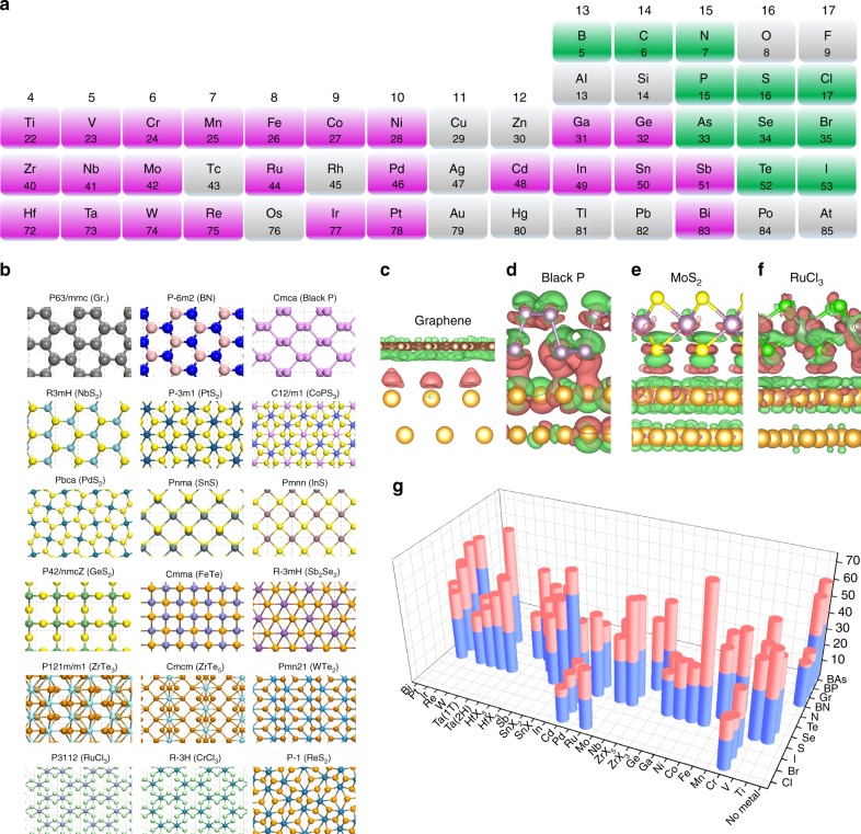
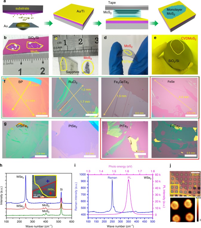
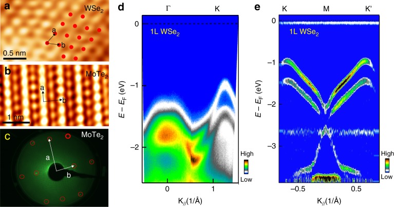
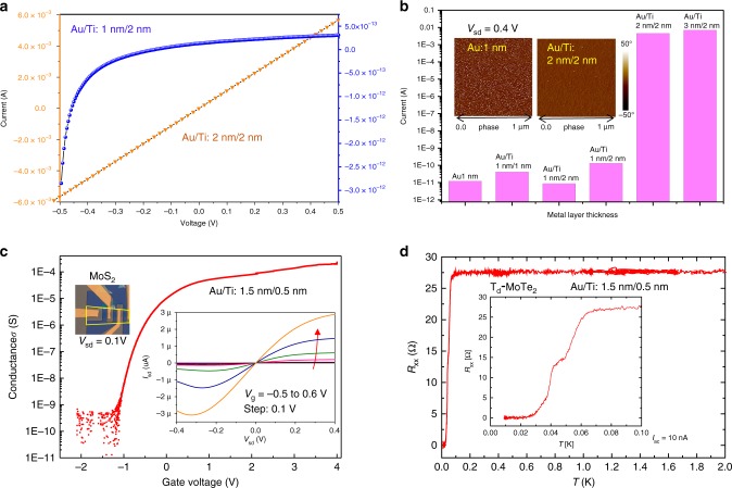
Two-dimensional materials provide extraordinary opportunities for exploring phenomena arising in atomically thin crystals. Beginning with the first isolation of graphene, mechanical exfoliation has been a key to provide high-quality two-dimensional materials, but despite improvements it is still limited in yield, lateral size and contamination. Here we introduce a contamination-free, one-step and universal Au-assisted mechanical exfoliation method and demonstrate its effectiveness by isolating 40 types of single-crystalline monolayers, including elemental two-dimensional crystals, metal-dichalcogenides, magnets and superconductors. Most of them are of millimeter-size and high-quality, as shown by transfer-free measurements of electron microscopy, photo spectroscopies and electrical transport. Large suspended two-dimensional crystals and heterojunctions were also prepared with high-yield. Enhanced adhesion between the crystals and the substrates enables such efficient exfoliation, for which we identify a gold-assisted exfoliation method that underpins a universal route for producing large-area monolayers and thus supports studies of fundamental properties and potential application of two-dimensional materials.


Conflict of interest statement

The authors declare the following competing interests that three Chinese patents were filed (201910529797.7; 201910529796.2; 201910529623.0) by the Institute of Physics, Chinese Academy of Sciences, along with their researchers (Y.H., H.L.L., and X.J.Z).

Figures

Fig. 1
Fig. 1. DFT calculated interlayer binding energies of 2D materials and adsorption energies on Au (111) surfaces.
a Part of the periodic table, showing the elements involved in most 2D materials between groups 4 (IVB) and 17 (VIIA). b Eighteen space groups and typical structural configurations (top views) of the 2D materials. cf DCD of four Au (111)/2D crystal interfaces with (non-metallic) terminating atoms between groups 14 (IVA) and 17 (VIIA). Isosurface values of these DCD plots are 5 × 10−4 e Bohr−3 (graphene), 1 × 10−2 e Bohr−3 (BP), and 1 × 10−3 e Bohr−3 (MoS2, RuCl3), respectively. g Bar graph comparing the interlayer binding energies of 2D materials (blue cylinders) with their adsorption energies on Au (111) (red cylinders). The visible red cylinders represent the difference between the Au/2D crystal interaction and the interlayer interaction.
Fig. 2
Fig. 2. Mechanical exfoliation of different monolayer materials with macroscopic size.
a Schematic of the exfoliation process. bd Optical images of exfoliated MoS2 on SiO2/Si, sapphire, and plastic film. e 2-inch CVD-grown monolayer MoS2 film transferred onto a 4 inch SiO2/Si substrate. fg Optical images of large exfoliated 2D crystals: BP, FeSe, Fe3GeTe2, RuCl3, PtSe2, PtTe2, PdTe2, and CrSiTe3. Those exfoliated monolayers highlighted in the red box are, so far, not accessible using other mechanical exfoliate method. h Optical image and Raman spectra of a MoS2/WSe2 heterostructure. i Raman and photoluminescence (PL) spectra of suspended monolayer WSe2. j Optical image of suspended WSe2 with different thicknesses (1 L to 3 L) and a PL intensity map of the suspended monolayer.
Fig. 3
Fig. 3. STM and ARPES measurements of 2D materials exfoliated onto conductive Au/Ti adhesion layers.
a, b STM images of monolayer WSe2 and Td-MoTe2, respectively. c LEED pattern of monolayer Td-MoTe2. d, e Band structure of monolayer WSe2. d Original ARPES band structure of monolayer WSe2 (hv = 21.2 eV) along Γ-K high symmetry line. The valence band maximum (VBM) is positioned at K instead of Γ, which is an important signature of monolayer WSe2. e Second-derivative spectra of band dispersion along K–M–K’, showing clear spin-orbital coupling (SOC) induced spin-splitting bands.
Fig. 4
Fig. 4. Electrical measurements of metal adhesion layers and of 2D materials exfoliated onto nonconductive metal films.
a Electrical transfer curves of typical Au/Ti adhesion layers. b Two-terminal resistance of Au/Ti layers with different nominal thickness. The inset shows atomic force microscope (AFM) phase maps of two metal layers. c Gate voltage-conductance transfer characteristics of a top-gated MoS2 FET on SiO2/Si with Au (1.5 nm)/Ti (0.5 nm) adhesion layer (T = 220 K, source−drain bias Vsd = 0.1 V). Left inset: Optical image of the FET device with windows for the ionic-liquid top gate. Right inset: low-bias source-drain current-voltage characteristics for gate voltage −0.5 to 0.6 V. d Temperature-dependent resistance of a Td-MoTe2 flake exfoliated onto SiO2/Si with a 2 nm metal adhesion layer.

References

    1. He SL, et al. Phase diagram and electronic indication of high-temperature superconductivity at 65 K in single-layer FeSe films. Nat. Mater. 2013;12:605–610. doi: 10.1038/nmat3648. - DOI - PubMed
    1. Zhang C, et al. Engineering point-defect states in monolayer WSe2. ACS Nano. 2019;13:1595–1602. - PubMed
    1. Ezawa M. Valley-polarized metals and quantum anomalous hall effect in silicene. Phys. Rev. Lett. 2012;109:055502. doi: 10.1103/PhysRevLett.109.055502. - DOI - PubMed
    1. Jiang SW, Li LZ, Wang ZF, Mak KF, Shan J. Controlling magnetism in 2D CrI3 by electrostatic doping. Nat. Nanotechnol. 2018;13:549–553. doi: 10.1038/s41565-018-0135-x. - DOI - PubMed
    1. Novoselov KS, et al. Electric field effect in atomically thin carbon films. Science. 2004;306:666–669. doi: 10.1126/science.1102896. - DOI - PubMed