. 2020 Jun 22;3(6):5552-5562.
doi: 10.1021/acsaem.0c00525. Epub 2020 May 8.

Rapid Scalable Processing of Tin Oxide Transport Layers for Perovskite Solar Cells

Affiliations

Rapid Scalable Processing of Tin Oxide Transport Layers for Perovskite Solar Cells

Joel A Smith et al. ACS Appl Energy Mater. .

Abstract

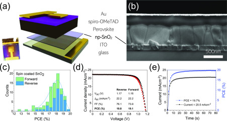
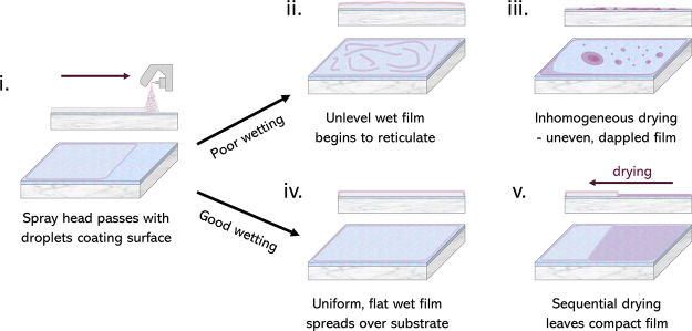
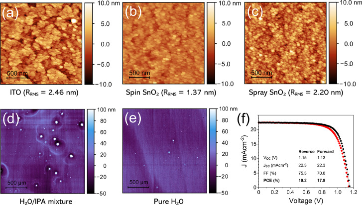
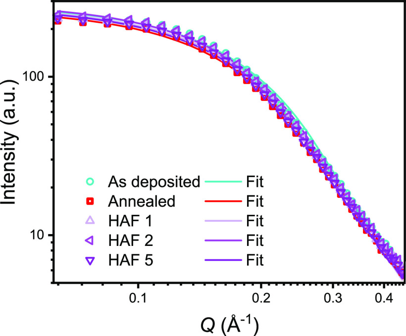
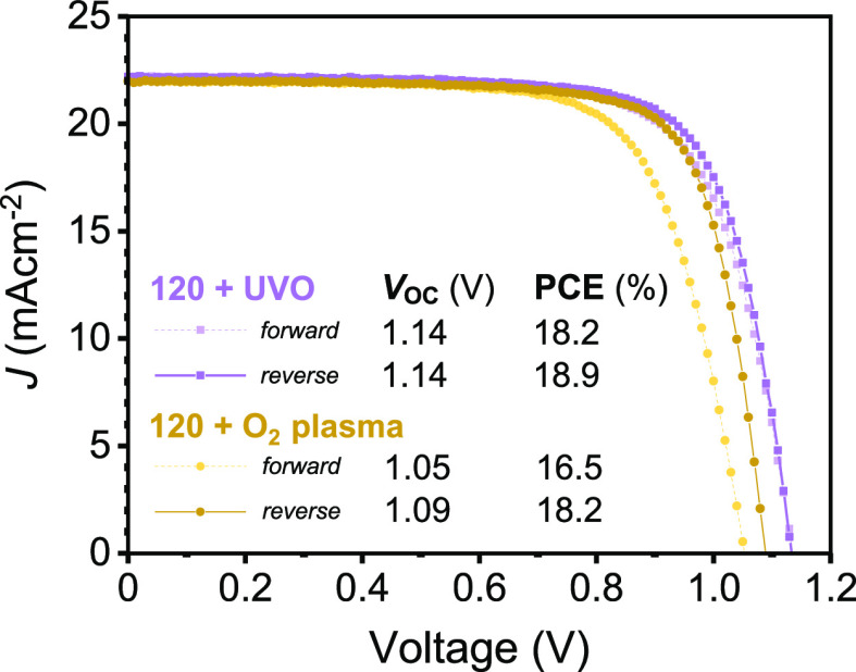
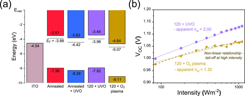
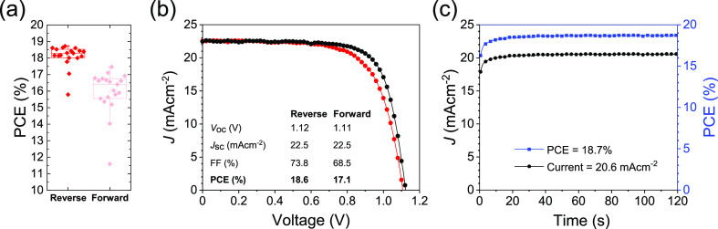
The development of scalable deposition methods for perovskite solar cell materials is critical to enable the commercialization of this nascent technology. Herein, we investigate the use and processing of nanoparticle SnO2 films as electron transport layers in perovskite solar cells and develop deposition methods for ultrasonic spray coating and slot-die coating, leading to photovoltaic device efficiencies over 19%. The effects of postprocessing treatments (thermal annealing, UV ozone, and O2 plasma) are then probed using structural and spectroscopic techniques to characterize the nature of the np-SnO2/perovskite interface. We show that a brief "hot air flow" method can be used to replace extended thermal annealing, confirming that this approach is compatible with high-throughput processing. Our results highlight the importance of interface management to minimize nonradiative losses and provide a deeper understanding of the processing requirements for large-area deposition of nanoparticle metal oxides.


Conflict of interest statement

The authors declare the following competing financial interest(s): D.G.L. is a co-director of the company Ossila that retail materials and equipment used in perovskite photovoltaic device research and development.

Figures

Figure 1
Figure 1
np-SnO2 device structure and performance. (a) Illustration of the n–i–p layer architecture with a photograph of a completed device inset. (b) Cross-sectional SEM image of a completed device showing densely packed perovskite grains and ultrathin np-SnO2 layer. (c) Histogram of all spin-coated device efficiencies (forward and reverse sweep), showing excellent reproducibility. Champion cell performance is illustrated by (d) a current–voltage sweep and (e) stabilized device performance at the JV determined MPP.
Figure 2
Figure 2
Scheme illustrating the optimized np-SnO2 drying process across the UVO-treated ITO surface: (i) spray-coating, (ii) fast reticulation, (iii) dry film with poor uniformity, (iv) ideal wet film, and (v) drying proceeds across the substrate.
Figure 3
Figure 3
AFM height maps for uniformity and roughness of (a) ITO, (b) spin-coated and (c) spray-coated np-SnO2 layers. Profilometric mapping of completed devices using spray-deposited np-SnO2 with (d) IPA/H2O mixed solvent and (e) H2O-only solution; here, np-SnO2 layer inhomogeneity in the IPA/H2O cast film leads to pinholes in subsequent layers. (f) JV curve for the best-performing spray np-SnO2 device.
Figure 4
Figure 4
In-plane linecuts and Guinier–Porod fitting of GISAXS from np-SnO2 layers with different annealing conditions; as-deposited, 30 min 150 °C annealed, and HAF for 1, 2, and 5 min. 2D GISAXS patterns for all samples are shown in Figure S13.
Figure 5
Figure 5
JV curves for the best-performing cells using np-SnO2 treated with 1 min 120 °C drying and either 15 min UVO or 5 min O2 plasma prior to perovskite deposition. Key sweep parameters are inset (full parameters in Table S4), with the O2 plasma-treated np-SnO2 device exhibiting lower VOC and increased hysteresis.
Figure 6
Figure 6
Understanding the effect of UVO and O2 plasma treatments. (a) Electronic structure at the np-SnO2 surface with the Fermi level (EF) from UPS measurements, valence band from UPS and XPS and estimated conduction band from the optical band gap. (b) Stabilized light-VOC measurements for 120 + UVO and 120 + O2 devices, showing reduced VOC for the plasma treatment. Apparent nid from linear fits are shown, and in the O2 plasma case, behavior indicates increased nonradiative recombination at the ETL interface.,
Figure 7
Figure 7
Photovoltaic performance for devices prepared using fast processing: spray coating, 1 min HAF, and UVO treatment. (a) Reverse and forward sweep efficiencies for 19 operational cells, (b) JV sweep, and (c) SPO of the best-performing cell.

References

    1. Kojima A.; Teshima K.; Shirai Y.; Miyasaka T. Organometal Halide Perovskites as Visible-Light Sensitizers for Photovoltaic Cells. J. Am. Chem. Soc. 2009, 131, 6050–6051. 10.1021/ja809598r. - DOI - PubMed
    1. NREL . Best Research-Cell Efficiencies. https://www.nrel.gov/pv/cell-efficiency.html (accessed Dec 10, 2019).
    1. Stranks S. D. Nonradiative Losses in Metal Halide Perovskites. ACS Energy Lett. 2017, 2, 1515–1525. 10.1021/acsenergylett.7b00239. - DOI
    1. Egger D. A.; Bera A.; Cahen D.; Hodes G.; Kirchartz T.; Kronik L.; Lovrincic R.; Rappe A. M.; Reichman D. R.; Yaffe O. What Remains Unexplained about the Properties of Halide Perovskites?. Adv. Mater. 2018, 30, 1800691.10.1002/adma.201800691. - DOI - PubMed
    1. Saliba M.; Matsui T.; Seo J.-Y.; Domanski K.; Correa-Baena J.-P.; Nazeeruddin M. K.; Zakeeruddin S. M.; Tress W.; Abate A.; Hagfeldt A.; Grätzel M. Cesium-Containing Triple Cation Perovskite Solar Cells: Improved Stability, Reproducibility and High Efficiency. Energy Environ. Sci. 2016, 9, 1989–1997. 10.1039/C5EE03874J. - DOI - PMC - PubMed