Review
. 2020 Jun 28;20(13):3624.
doi: 10.3390/s20133624.

Motion Detection Using Tactile Sensors Based on Pressure-Sensitive Transistor Arrays

Affiliations
Review

Motion Detection Using Tactile Sensors Based on Pressure-Sensitive Transistor Arrays

Jiuk Jang et al. Sensors (Basel). .

Abstract

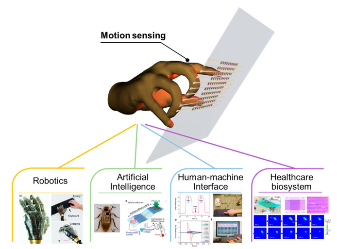
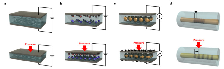
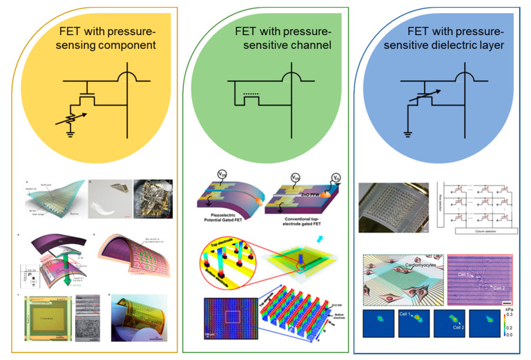
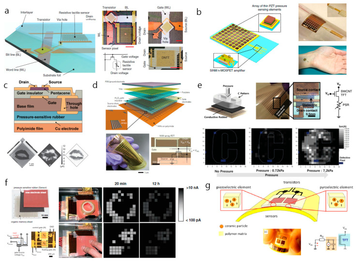
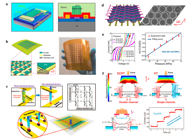
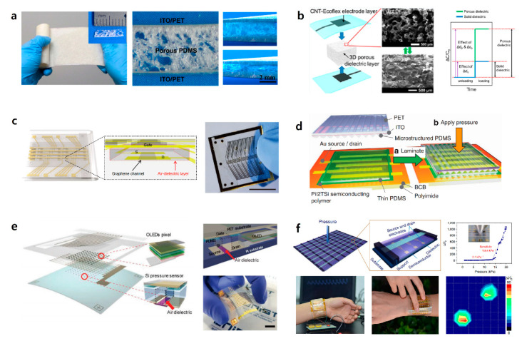
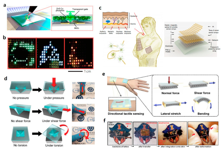
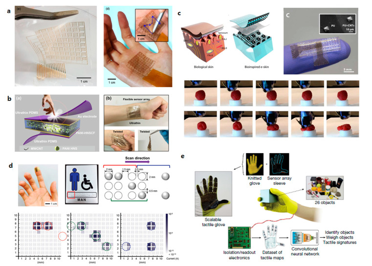
In recent years, to develop more spontaneous and instant interfaces between a system and users, technology has evolved toward designing efficient and simple gesture recognition (GR) techniques. As a tool for acquiring human motion, a tactile sensor system, which converts the human touch signal into a single datum and executes a command by translating a bundle of data into a text language or triggering a preset sequence as a haptic motion, has been developed. The tactile sensor aims to collect comprehensive data on various motions, from the touch of a fingertip to large body movements. The sensor devices have different characteristics that are important for target applications. Furthermore, devices can be fabricated using various principles, and include piezoelectric, capacitive, piezoresistive, and field-effect transistor types, depending on the parameters to be achieved. Here, we introduce tactile sensors consisting of field-effect transistors (FETs). GR requires a process involving the acquisition of a large amount of data in an array rather than a single sensor, suggesting the importance of fabricating a tactile sensor as an array. In this case, an FET-type pressure sensor can exploit the advantages of active-matrix sensor arrays that allow high-array uniformity, high spatial contrast, and facile integration with electrical circuitry. We envision that tactile sensors based on FETs will be beneficial for GR as well as future applications, and these sensors will provide substantial opportunities for next-generation motion sensing systems.

Keywords: gesture recognition; pressure sensor; tactile sensor; transistor.


Conflict of interest statement

The authors declare no conflict of interest.

Figures

Figure 1
Figure 1
Tactile sensors for motion sensing. Reproduced with permission [24]. Copyright 2014, Springer Nature. Reproduced with permission [9]. Copyright 2018, American Association for the Advancement of Science. Reproduced with permission [10]. Copyright 2015, American Chemical Society. Reproduced with permission [25]. Copyright 2020, American Chemical Society.
Figure 2
Figure 2
Schematic illustrations of transduction mechanisms of tactile sensors: (a) piezoresistivity; (b) capacitance; (c) piezoelectricity; (d) optics.
Figure 3
Figure 3
Representative tactile sensor arrays with active-matrix driving with circuits. Reproduced with permission [63]. Copyright 2013, Springer Nature. Reproduced with permission [64]. Copyright 2019, Springer Nature. Reproduced with permission [65]. Copyright 2010, Elsevier. Reproduced with permission [66]. Copyright 2013, American Association for the Advancement of Science. Reproduced with permission [67]. Copyright 2017, Springer Nature. Reproduced with permission [15]. Copyright 2020, American Chemical Society.
Figure 4
Figure 4
Field-effect transistor (FET)-based tactile sensor arrays with pressure-sensing components. (a) Active-matrix tactile pixel sensor comprising a switching transistor and a resistive touch sensor. (b) Thin conformal array pressure sensor made of elements of zirconate titanate (PZT) with transistor amplified pressure-sensing capability. (c) Tactile pressure sensor with pressure-sensitive component in its active-matrix transistor array. (d) Nanowire-based flexible tactile pressure sensor with pressure-sensitive rubber (PSR)-integrated active-matrix transistor array. (e) Tactile pressure sensor with carbon nanotube backplane integrated with active-matrix transistor array. (f) Nonvolatile tactile pressure sensor with active-matrix two-transistor array with intermediate pressure-sensitive rubber sheet. (g) Bifunctional sensor array with flexible ceramic polymer sensor laminated onto transistor backplane. (a) Reproduced with permission [80]. Copyright 2013, Springer Nature. (b) Reproduced with permission [79]. Copyright 2014, Springer Nature. (c) Reproduced with permission [62]. Copyright 2004, National Academy of Sciences. (d) Reproduced with permission [81]. Copyright 2010, Springer Nature. (e) Reproduced with permission [82]. Copyright 2015, John Wiley and Sons. (f) Reproduced with permission [84]. Copyright 2009, The American Association for the Advancement of Science. (g) Reproduced with permission [83]. Copyright 2009, Journal of Applied Physics.
Figure 5
Figure 5
Transistor array using pressure-sensitive channel materials. (a) Schematic illustration of a FET based on a MoS2 and ZnO heterostructure (left). Schematic cartoon graphs of the architecture of the device that uses the ZnO nanowire (NW) array and MoS2 flake, separated by a 20-nm atomic layer deposition (ALD)-deposited Al2O3 layer. (b) Schematic of a 10 × 10 tribotronic transistor array (TTA) (left). Partial enlarged tilted views of the TTA configuration and pixel structure, respectively (inset). Optical photograph of a fully integrated TTA with each sensing pixel of 5 × 5 mm (right). (c) Comparison between three-terminal voltage-gated NW FET and two-terminal strain-gated vertical piezotronic transistor (left). Color gradient in the strained strain-gated vertical piezotronic transistor (SGVPT) represents the strain-induced piezopotential field, in which red and blue indicate positive and negative piezopotential, respectively. ZnO NWs in SGVPT grow along the c axis (red arrow). Equivalent circuit diagram of the 3D SGVPT array (right). Equivalent circuit diagram of the 3D SGVPT array (bottom). The region highlighted by black dashed lines is the unit SGVPT device, in which εg represents the mechanical strain gate signal and the vertical dotted line between the two terminals of the SGVPT denotes the modulation effect of εg on the conducting characteristics of the device. (d) Schematic illustration of a 2D piezotronic transistor (2DPT) array using ZnO nanoplatelet (left). Scanning electron micrograph of 2DPT array with high spatial resolution (≈12,700 dpi) (right). (e) The modulation of carrier transport by pressure in a piezotronic transistor based on ZnO twin nanoplatelets, which shows the characteristic of piezotronic effect (left). ln(I)−P curve demonstrates a linear relationship between ln(I) and the applied pressure, showing the extreme sensitivity and indicating the modulation effect of applied pressure on conductance (right). (f) Piezopotential distributions and the corresponding energy-band diagrams of double-channel piezotronic transistor (DCPT) and conventional piezotronic transistor (PT) (top). Compared to one rise and another drop in conventional PT, both Schottky barriers in DCPT decrease with increasing pressure. Energy-band diagram of DCPT without (black dashed line) and with (red line) piezotronic effect, in which ΔEimage and ΔEpiezo represent mirror force and piezopotential-induced Schottky barrier height change, respectively (left). Current increased step-by-step with increasing pressure by a step of 63.5 kPa from 0.75 to 1.00 MPa at a fixed bias (right). (a) Reproduced with permission [86]. Copyright 2016, American Chemical Society (b) Reproduced with permission [89]. Copyright 2016, American Chemical Society. (c) Reproduced with permission [66]. Copyright 2013, American Association for the Advancement of Science. (d) Reproduced with permission [91]. Copyright 2017, American Chemical Society. (e) Reproduced with permission [88]. Copyright 2017, American Chemical Society. (f) Reproduced with permission [92]. Copyright 2018, American Chemical Society.
Figure 6
Figure 6
Results of dielectric layer modification. (a) The photo image of the fabricated large area microstructured polydimethylsiloxane (PDMS) film (the inset shows the cross-sectional photo image of the microstructured PDMS film) (left); The cross-sectional photo images of the microstructured PDMS film clipped by a tweezer without pressure (upper) and with pressure (bottom) (right). (b) Relative changes in the capacitances of pressure sensors using solid and porous elastomeric dielectric layers induced by identical levels of external loading. The synergy of the larger deformation by the reduced stiffness and the increased effective dielectric constant by the closure of the air gap dramatically amplifies the capacitance change. (c) Schematic images of pressure-sensitive graphene FETs with air-dielectric layers after the folding. The air-dielectric layer is placed between the graphene channel and the gate electrode as illustrated in the schematic image (inset) (left); Photograph of the fabricated pressure-sensitive graphene FETs; scale bar, 1 cm (right). (d) Schematic of the final fabrication step of our pressure-sensitive transistor. (e) Schematic of active-matrix pressure-sensitive display, integrating the Si tactile pressure sensors and organic light-emitting diodes (OLEDs). (f) Suspended gate organic thin-film transistor pressure sensors. (a) Reproduced with permission [94]. (b) Reproduced with permission [95]. Copyright 2016, ACS Applied Materials & Interfaces. (c) Reproduced with permission [67]. Copyright 2017, Nature Communications. (d) Reproduced with permission [93]. Copyright 2013, Nature Communications. (e) Reproduced with permission [16]. Copyright 2019, Advanced Material Technologies. (f) Reproduced with permission [96]. Copyright 2015, Nature Communications.
Figure 7
Figure 7
Multimodal, multifunctional tactile sensor arrays based on FETs. (a) Schematic layouts of the pressure-sensor array integrated with ZnS:Cu phosphor particles. (b) Green, blue, and red color interactive e-skins are used to spatially map and display the pressure applied with C-(left), A-(center) and L-(right) shaped PDMS slabs, respectively. (c) Skin-inspired highly stretchable and conformable matrix networks; a schematic illustration of stretchable and conformable matrix networks (SCMNs) conforming to the surface of a human arm and an expanded network (expansion: 200%) conforming to the surface of a human abdomen (right); the tree branch-like connections of neurons (left bottom); the sensory receptors of the glabrous skin (left top). (d) Schematic illustrations without stimulus and under three different mechanical stimuli for pressure, shear force, and torsion. There were possible geometric deformations of the pyramid-plug structure with mechanical loadings. (e) Schematic of a stress-direction-sensitive electronic skin for the detection and differentiation of various mechanical stimuli including normal, shear, stretching, bending, and twisting forces. (f) A commercial temporary transfer tattoo provides an alternative to polyester/polyvinyl alcohol (PVA) for the substrate; in this case, the system includes an adhesive to improve bonding to the skin. Images are of the back side of a tattoo (far left), electronics integrated onto this surface (middle left), and attached to the skin with electronics facing down in undeformed (middle right) and compressed (far right) states. (a) Reproduced with permission [15]. Copyright 2020, Nano Letters. (b) Reproduced with permission [64]. Copyright 2013, Nature Materials. (c) Reproduced with permission [99]. Copyright 2018, Nature Communications. (d) Reproduced with permission [101]. Copyright 2019, Advanced Materials Technologies. (e) Reproduced with permission [102]. Copyright 2014, ACS Nano. (f) Reproduced with permission [103]. Copyright 2011, Science.
Figure 8
Figure 8
Tactile pressure sensors for e-skin and robotics. (a) Photograph of the large area flexible active-matrix (AM) MOS2 tactile sensor array (left). Photograph of the AM MoS2 tactile sensor on the human palm (right). (b) Primary design concept of flexible e-skin sensor based on polyaniline hollow nanosphere composite films (PANI-HNSCF) (left). Optical image of a wearable ultrathin e-skin sensor array on the wrist and under various mechanical deformations (right). (c) Cross-section of the skin of the fingertip depicting key sensory structures and soft biomimetic e-skin (left). Optical image showing carbon nanotube-polyurethane (CNT-PU) interconnects for signal recording with inductance/capacitance ratio (LCR) meter and SEM picture of the top e-skin layer with molded pyramids (right), showing CNT-PU and PU areas (inset). Tactile feedback prevented flattening of the raspberry. Without tactile feedback, the fruit was crushed (bottom). (d) Digital image of the flexible tactile array sensor attached to the tip of an index finger as an artificial fingertip (left). Digital image of a braille sign stating “restroom for handicapped males” (middle). Illustration denoting the dimensions of the scanned braille (right). Current profiles obtained from the artificial fingertip while scanning the braille (bottom). (e) The scalable tactile glove (STAG) consists of a sensor array with 548 elements covering the entire hand, attached to a custom knit glove. An electrical readout circuit is used to acquire the normal force recorded by each sensor at approximately 7.3 fps. Using this setup allows recording of a dataset of 135,187 tactile maps while interacting with 26 different objects. A deep convolutional neural network trained purely on tactile information can be used to identify or weigh objects and explore the tactile signatures of the human grasp. The glove shown at the center is a rendering. (a) Reproduced with permission [117]. Copyright 2019, American Chemical Society. (b) Reproduced with permission [118]. Copyright 2017, Elsevier. (c) Reproduced with permission [119]. Copyright 2018, American Association for the Advancement of Science. (d) Reproduced with permission [120]. Copyright 2018, John Wiley and Sons. (e) Reproduced with permission [121]. Copyright 2019, Springer Nature.

References

    1. Wu Y., Huang T.S. Vision-Based Gesture Recognition: A review; Proceedings of the Gesture-Based Communication in Human-Computer Interaction; Berlin/Heidelberg, Germany. 17 March 1999; pp. 103–115.
    1. Jeon C., Kwon O.J., Shin D., Shin D. Hand-Mouse Interface Using Virtual Monitor Concept for Natural Interaction. IEEE Access. 2017;5:25181–25188. doi: 10.1109/ACCESS.2017.2768405. - DOI
    1. Dorner B., Hagen E. Towards an American Sign Language Interface; Proceedings of the Integration of Natural Language and Vision Processing: Computational Models and Systems; Dordrecht, The Netherlands. 31 July 1995; pp. 143–161.
    1. An B.W., Shin J.H., Kim S.-Y., Kim J., Ji S., Park J., Lee Y., Jang J., Park Y.-G., Cho E., et al. Smart Sensor Systems for Wearable Electronic Devices. Polymers. 2017;9:303. doi: 10.3390/polym9080303. - DOI - PMC - PubMed
    1. Park Y.G., Lee S., Park J.U. Recent Progress in Wireless Sensors for Wearable Electronics. Sensors. 2019;19:4353. doi: 10.3390/s19204353. - DOI - PMC - PubMed