

Templated-Assembly of CsPbBr3 Perovskite Nanocrystals into 2D Photonic Supercrystals with Amplified Spontaneous Emission
- PMID: 32608040
- PMCID: PMC7540499
- DOI: 10.1002/anie.202006152
Templated-Assembly of CsPbBr3 Perovskite Nanocrystals into 2D Photonic Supercrystals with Amplified Spontaneous Emission
Abstract
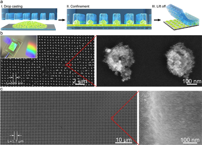
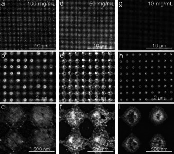
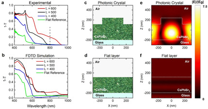
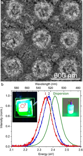
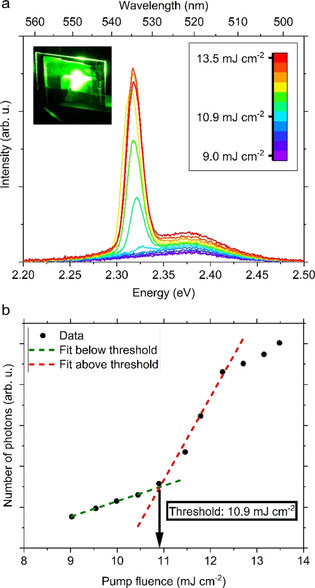
Perovskite nanocrystals (NCs) have revolutionized optoelectronic devices because of their versatile optical properties. However, controlling and extending these functionalities often requires a light-management strategy involving additional processing steps. Herein, we introduce a simple approach to shape perovskite nanocrystals (NC) into photonic architectures that provide light management by directly shaping the active material. Pre-patterned polydimethylsiloxane (PDMS) templates are used for the template-induced self-assembly of 10 nm CsPbBr3 perovskite NC colloids into large area (1 cm2 ) 2D photonic crystals with tunable lattice spacing, ranging from 400 nm up to several microns. The photonic crystal arrangement facilitates efficient light coupling to the nanocrystal layer, thereby increasing the electric field intensity within the perovskite film. As a result, CsPbBr3 2D photonic crystals show amplified spontaneous emission (ASE) under lower optical excitation fluences in the near-IR, in contrast to equivalent flat NC films prepared using the same colloidal ink. This improvement is attributed to the enhanced multi-photon absorption caused by light trapping in the photonic crystal.
Keywords: 2D photonic crystals; PDMS template; amplified spontaneous emission (ASE); perovskite nanocrystals; self-assembly.
© 2020 The Authors. Published by Wiley-VCH GmbH.
Conflict of interest statement
The authors declare no conflict of interest.
Figures
References
-
- None
-
- Huang H., Polavarapu L., Sichert J. A., Susha A. S., Urban A. S., Rogach A. L., NPG Asia Mater. 2016, 8, e328;
-
- Akkerman Q. A., Rainò G., Kovalenko M. V., Manna L., Nat. Mater. 2018, 17, 394–405; - PubMed
-
- Li X., Cao F., Yu D., Chen J., Sun Z., Shen Y., Zhu Y., Wang L., Wei Y., Wu Y., Zeng H., Small 2017, 13, 1603996; - PubMed
Grants and funding
- Solar Technologies go Hybrid (SolTech)/Bayerisches Staatsministerium für Wissenschaft, Forschung und Kunst
- EXC 2089/1-390776260 ("e-conversion")/Deutsche Forschungsgemeinschaft
- SEV-2015-0496/Ministerio de Economía, Industria y Competitividad, Gobierno de España
- MDM-2017-0720/Spanish MINECO (Ministerio de Economía, Industria y Competitividad)
- 637116, ENLIGHTMENT/H2020 European Research Council
LinkOut - more resources
Full Text Sources
Research Materials
