Review
. 2020 Jul 6;7(1):23.
doi: 10.1186/s40580-020-00232-9.

Laser digital patterning of conductive electrodes using metal oxide nanomaterials

Affiliations
Review

Laser digital patterning of conductive electrodes using metal oxide nanomaterials

Vu Binh Nam et al. Nano Converg. .

Abstract

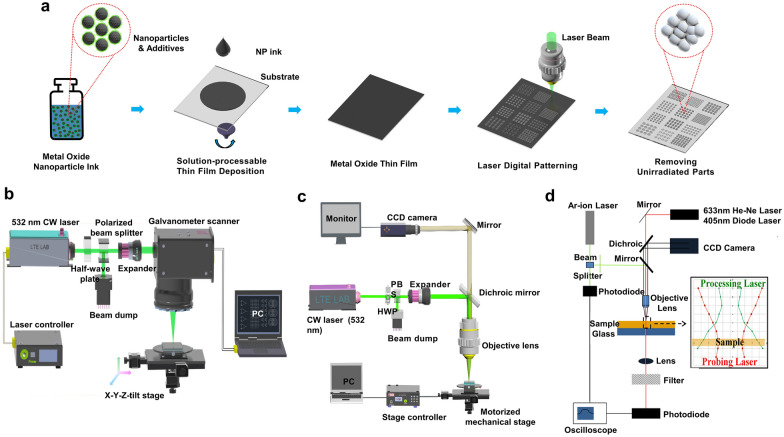
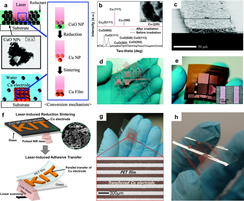
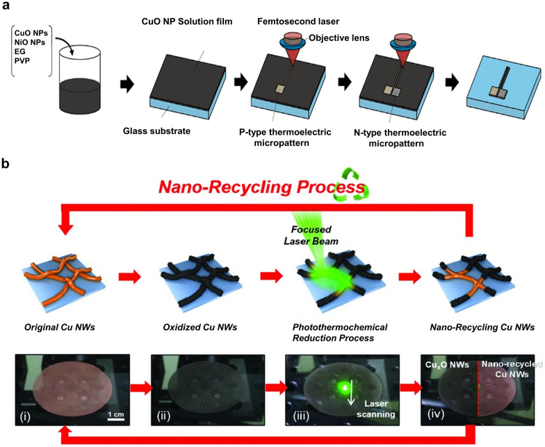
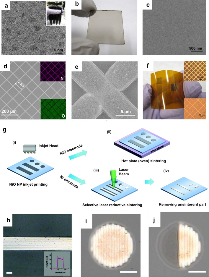
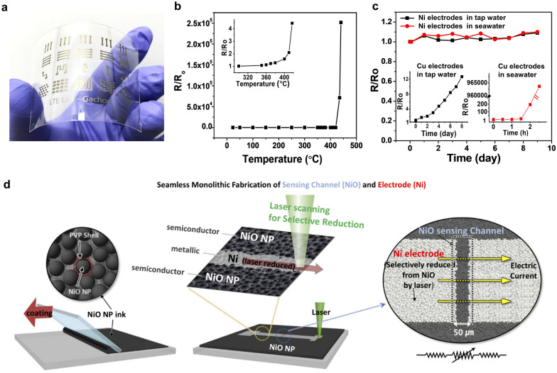
As an alternative approach to the conventional deposition and photolithographic processes, the laser digital patterning (LDP) process, which is also known as the laser direct writing process, has attracted considerable attention because it is a non-photolithographic, non-vacuum, on-demand, and cost-effective electrode fabrication route that can be applied to various substrates, including heat-sensitive flexible substrates. The LDP process was initially developed using noble metal nanoparticles (NPs) such as Au and Ag because such materials are free from oxidation even in a nanosize configuration. Thus, the NPs must be fused together to form continuous conductive structures upon laser irradiation. However, common metals are easily oxidized at the nanoscale and exist in oxidized forms owing to the extremely large surface-to-volume ratio of NPs. Therefore, to fabricate conductive electrodes using common metal NPs via the LDP process, laser irradiation should be used to sinter the NPs and simultaneously induce additional photochemical reactions, such as reduction, and defect structure modification to increase the conductivity of the electrodes. This review summarizes recent studies on the LDP process in which metal oxide NPs, such as ITO, ZnO, CuO, and NiO, were exclusively utilized for fabricating conductive electrodes. The outlook of the LDP process for these materials is also discussed as a method that can be used together with or as a replacement for conventional ones to produce next-generation transparent conductors, sensors, and electronics.

Keywords: CuO; Digital patterning; ITO; Laser; NiO; Reductive sintering; ZnO.


Conflict of interest statement

The authors declare that they have no competing interests.

Figures

Fig. 1
Fig. 1
a Schematic of the overall procedure of the LDP process. b Schematic of the laser setup for moving the laser beam using a galvano mirror scanner. c Schematic of the laser setup for a fixed laser beam through an objective lens (Figures b and c reproduced with permission from Ref. [20]. Copyright Wiley–VCH, 2019). d Schematic of the laser setup for integration of a processing laser and a probing laser (Figure d reproduced with permission from Ref. [10]. Copyright Springer, 2015)
Fig. 2
Fig. 2
a Variation of the electrical resistivity (sheet resistance) of the laser-irradiated ITO film depending on the laser fluence of a single pulse. b Optical image to compare the transparency of thin films after the laser process (i: bare PET; ii: ITO film only; iii: ITO film after a single laser pulse at 80 mJ cm−2; iv: ITO film after a single laser pulse at 140 mJ cm−2) (a and b reproduced with the permission from Ref. [30]. Copyright Elsevier, 2015). c Optical transmission spectra of ITO thin films with different incident laser fluences. d Photographic image of a gravure-printed ITO film irradiated within the areas indicated by the black lines at different laser fluences (i: 0.49 J m−2; ii: 0.56 J m−2; iii: 0.65 Jm−2). Paper with millimeter squares was used as a background (Figures c and d reproduced with permission from Ref. [33], Copyright Nature Publishing Group, 2019). e Dependence of the sheet resistance of the laser-annealed ITO NP thin film on air–Ar mixed background gas in a quartz enclosure. f Transmittance data for a laser-annealed ITO NP thin film measured under different air flows with a fixed Ar flow at 8000 mL/min (e and f reproduced with permission from Ref. [29]. Copyright Springer, 2011)
Fig. 3
Fig. 3
a Schematic side view of the excimer laser annealing process and the ZnO NP field-effect transistor structure. S and D indicate the source and drain electrodes, respectively. The top right inset presents a top-view SEM image of transistor electrodes with a layer of deposited ZnO NPs. b Transmission electron microscopy (TEM) image of the ZnO NP film after excimer laser irradiation. The inset shows the diffraction pattern for the marked region. c Room-temperature photoluminescence spectra of the ZnO thin film with and without laser annealing (ac reproduced with permission from Ref. [42]. Copyright Springer, 2009). d Sheet resistance of the ZnO thin film depending on the background gas during laser annealing. e Transmittance of ZnO thin films annealed in background gases with different compositions. f Optical microscope image of 1.5-µm-line width patterns generated on the ZnO thin film (df reproduced with permission from Ref. [44]. Copyright Springer, 2012)
Fig. 4
Fig. 4
a Technical illustration and schematics of the laser printing process to generate Zn electrodes on Na-CMC. b Schematic of the laser-printed resistive Zn strain gauge. Response of the strain gauge under deflection. c Photograph of the dissolution process of Zn patterns on the Na-CMC substrate in distilled water (ac reproduced with permission from Ref. [55]. Copyright Wiley–VCH 2017)
Fig. 5
Fig. 5
a Schematic of the proposed process for the conversion of CuO NPs into a Cu film via photochemical reduction and photothermal agglomeration. b XRD analysis results obtained before and after laser irradiation; (inset) TEM image of a Cu film processed using a pulsed laser. c Cross-sectional SEM image of the Cu electrode. d, e Photograph of Cu electrode patterns on a glass substrate and a PI substrate, respectively (ae reproduced with permission from Ref. [77]. Copyright American Chemical Society 2011). f Schematic of the fabrication procedures for laser-induced reductive sintering and laser-induced adhesive transfer. g Photograph and microscope image of Cu NP electrodes transferred to a PET receiver film at a laser power of 2 W and a laser scanning speed of 2000 mm min−1. h Photograph of arbitrary Cu electrode patterns transferred to the PET film (fh reproduced with permission from Ref. [81]. Copyright Elsevier, 2018)
Fig. 6
Fig. 6
a Selective fabrication of p- and n-type thermoelectric micropatterns via the reduction of CuO–NiO mixed NPs using femtosecond laser pulses. (Reproduced with permission from Ref. [83]. Copyright Springer, 2017). b Schematic of the nano-recycling process flow, with optical photographs corresponding to each stage of nano-recycling (Figures reproduced with permission from Ref. [85]. Copyright Wiley–VCH, 2015)
Fig. 7
Fig. 7
a TEM image of synthesized NiOx NPs. b Spin-coated NiOx thin film on a glass substrate. c SEM image of the surface of the NiOx film shown in b. d, e Top-view SEM images of mesh-type electrodes with different magnifications. The insets in d show elemental mapping images obtained via energy-dispersive X-ray spectroscopy. f Mesh-type Ni electrodes with different pitches on a PI substrate. The top and bottom insets show bright-field microscopic images of the mesh patterns generated with 20- and 80-μm pitches, respectively (af reproduced with permission from Ref. [105]. Copyright American Chemical Society 2014). g Schematics of the overall experimental procedures of the NiO NP inkjet printing and sintering processes; (i) NiO inkjet printing, (ii) hotplate (oven) sintering for NiO electrodes, (iii) selective laser reductive sintering for Ni electrodes, and (iv) removal of un-sintered parts via washing. h Photographs of Ni patterns formed by laser reductive sintering after washing to remove non-irradiated parts. The inset shows a cross-sectional profile of the Ni pattern. i, j Single dot of Ni and Ni/NiO hybrid electrode, respectively, obtained via laser reductive sintering. The scale bars indicate 20 μm (gj reproduced with permission from Ref. [108]. Copyright Royal Society of Chemistry, 2016)
Fig. 8
Fig. 8
a Customized Ni conductor patterns on a PET substrate. b Relative resistance variation (R/Ro) with an increase in the temperature from room temperature to 440 °C. The inset shows a magnified view in the temperature range of 300–420 °C. c Measured R/Ro of Ni electrodes in tap water and seawater. The insets show the measured R/Ro values of the Cu electrodes in tap water (left) and seawater (right) (ac reproduced with permission from Ref. [20]. Copyright Wiley–VCH, 2019). d Schematic of the monolithic LRS process. NiO NP ink is coated on a substrate via the doctor blading technique. Selective laser irradiation of the dried NiO layer using a computer-aided galvano-mirror system and a monolithic Ni-NiO–Ni structure having a NiO-channel (several tens of micrometers wide) formed via the simple hatching technique (d reproduced with permission from Ref. [109]. Copyright Wiley–VCH, 2020)

References

    1. Torii S, Yang W-J. J. Heat Mass Transf. 2005;48:537–544.
    1. Mustafeez W, Lee D, Grigoropoulos C, Salleo A. Opt. Express. 2011;19:15452–15458. - PubMed
    1. Yeo J, Hong S, Wanit M, Kang HW, Lee D, Grigoropoulos CP, Sung HJ, Ko SH. Adv. Funct. Mater. 2013;23:3316–3323.
    1. In JB, Lee D, Fornasiero F, Noy A, Grigoropoulos CP. ACS Nano. 2012;6:7858–7866. - PubMed
    1. Chung J, Lu H, Ou X, Zhou H, Yang C. Biomed. Opt. Express. 2016;7:4787–4802. - PMC - PubMed

LinkOut - more resources