Review
. 2020 Jul 10;13(14):3089.
doi: 10.3390/ma13143089.

Holography and Coherent Diffraction Imaging with Low-(30-250 eV) and High-(80-300 keV) Energy Electrons: History, Principles, and Recent Trends

Affiliations
Review

Holography and Coherent Diffraction Imaging with Low-(30-250 eV) and High-(80-300 keV) Energy Electrons: History, Principles, and Recent Trends

Tatiana Latychevskaia. Materials (Basel). .

Abstract

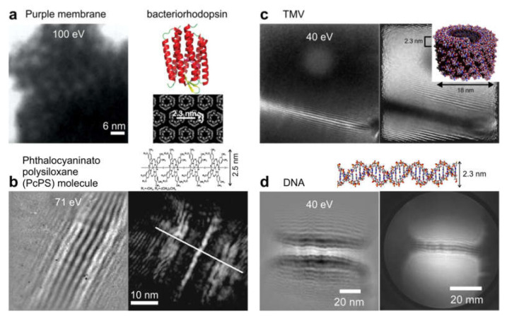
In this paper, we present the theoretical background to electron scattering in an atomic potential and the differences between low- and high-energy electrons interacting with matter. We discuss several interferometric techniques that can be realized with low- and high-energy electrons and which can be applied to the imaging of non-crystalline samples and individual macromolecules, including in-line holography, point projection microscopy, off-axis holography, and coherent diffraction imaging. The advantages of using low- and high-energy electrons for particular experiments are examined, and experimental schemes for holography and coherent diffraction imaging are compared.

Keywords: biomolecules; coherent diffraction imaging; diffraction; electron holography; holography; in-line holography; iterative phase retrieval.


Conflict of interest statement

The authors declare no conflict of interest.

Figures

Figure 1
Figure 1
Schematic of the electron scattering event and illustration of the symbols used. k0 and k are the wave vectors of the incident plane wave and the scattered wave, respectively, and ϑ is the scattering angle.
Figure 2
Figure 2
Differential scattering cross-sections dσ/dΩ of 150 eV and 200 keV electrons scattered by C and Au atoms, calculated as a function of the scattering angle ϑ. The units for the differential cross-sections are a02/sr, where a0 is the Bohr radius.
Figure 3
Figure 3
Inelastic mean free path (IMFP) as a function of electron energy. (a) IMFP calculated according to Equation (21). (b) IMFP measured based on the transmission of an electron beam through a thin amorphous carbon film as a function of the kinetic energy of the electron beam, using a transmission energy loss spectrometer [5]. Continuous lines are theoretical predictions for the IMFP by Ashley [6] and Penn [7], respectively; reprinted from [5], with permission from Elsevier.
Figure 4
Figure 4
Schematic illustrating the object phase, exit wave, and phase problem.
Figure 5
Figure 5
Calculated projected potentials for C and Au atoms (a), relative phase shifts introduced by C and Au atoms when probed with 150 eV (b), and 200 keV (c) electrons.
Figure 6
Figure 6
Schematic of symbols used in the Huygens-Fresnel principle, and the Fresnel and Fraunhofer diffraction integrals.
Figure 7
Figure 7
Images of the tobacco mosaic virus obtained by Gustav Kausche, Edgar Pfankuch, and Helmut Ruska in 1939, using an electron microscope. Reprinted from [22] by permission from Springer Nature, copyright 1939.
Figure 8
Figure 8
Principle of holography, as illustrated by Dennis Gabor [25,26]. (a,c) schematic of realization of holography in a transmission electron microscope. (b) Sample (left) with three words written on a transparent film, its hologram (middle) recorded on photographic film, and the reconstructed hologram (right) as a result of optical holography experiments involving recording and reconstruction of holograms, as shown in (d). (a,b) Reprinted from [25] by permission from Springer Nature, copyright 1948.
Figure 9
Figure 9
Images of a copper grid obtained by Morton and Ramberg using point projection microscopy (PPM) with electrons, at magnifications of (a) 200, (b) 600, and (c) 3000 times. Figure reprinted from [27], copyright (1939) by the American Physical Society.
Figure 10
Figure 10
Point projection microscopy (PPM) and in-line holography. (a) Experimental arrangement for PPM and the resulting image. (b) Experimental arrangement for in-line holography and the resulting image.
Figure 11
Figure 11
A biprism in an electron microscope. Ray diagrams for (a) an optical prism and (b) an electron biprism in an electron microscope. (c) Experimentally recorded electron biprism interference patterns with different potentials applied to the biprism, using a wire 2 μm in diameter. Reprinted from [39] by permission from Springer Nature, copyright 1956.
Figure 12
Figure 12
Off-axis electron holography. (a) Experimental arrangement. (b) Off-axis electron hologram exhibiting the shift in the interference pattern caused by the different thicknesses of the sample, and therefore by the differences in potential and the additional phase shift. Reprinted from [40] by permission from Springer Nature, copyright 1957.
Figure 13
Figure 13
Electron off-axis hologram of a latex sphere and its reconstruction. (a) Off-axis hologram of a latex sphere recorded at 200 keV, with Fresnel fringes from the biprism filament edge readily visible. (b) Amplitude of the Fourier spectrum of the hologram shown in (a). (c) Reconstructed amplitude. (d) Unwrapped reconstructed phase, with phase values between 0 and 13 rad. Reprinted from [53], with permission from Elsevier.
Figure 14
Figure 14
Low-energy electron off-axis holography. (a) Schematic arrangement of the low-energy holographic electron microscope with a biprism. (bd) Imaging of a perforated carbon foil: (b) off-axis hologram, (c) in-line hologram without biprism, and (d) amplitude reconstructed from (b). The field of view is 217 nm. Figure reprinted from [56], copyright (1996) by the American Physical Society.
Figure 15
Figure 15
Defocused imaging in TEM. (ac) Ray diagrams of a lens system when imaging (a) in focus, (b) under focus, and (c) over focus. The detector is at the same position in all three cases. The position of the object is shifted along the optical axis in (b) by Δf>0 and in (c) by Δf<0, and as a result, the image on the detector appears under-focused in (b) and over-focused in (c). (d) Under- and over-focused images of a pure phase object, a cat-shaped hole in a carbon film with the phase distribution shown in (e). (fh) show profiles through the middle of the 2D distribution of (f) the sample, (g) its first derivative, and (h) its second derivative.
Figure 16
Figure 16
Defocus series in transmission electron microscope (TEM). (a) Drawing of a holographic in-line scheme, where the red (yellow) color represents the object (reference) wave and Δf is the defocus distance. (be) Experimental in-line holograms of a latex sphere recorded at different values of defocus. (f) Amplitude and (g) phase of the object wave, reconstructed using an iterative flux-preserving focal series reconstruction algorithm [71]. Reprinted from [53], with permission from Elsevier.
Figure 17
Figure 17
In-line hologram of a latex sphere and its reconstruction. (a) In-line electron hologram of the latex sphere recorded at the defocus 180 μm, with 200 keV electrons in a TEM. The blue lines mark the area outside of which the transmission was set to 1 during the iterative reconstruction (support). (b,c) show the retrieved amplitude and phase distributions, respectively. Reprinted from [53], with permission from Elsevier.
Figure 18
Figure 18
Experimental arrangement for in-line holography with low-energy electrons.
Figure 19
Figure 19
Optical hologram of a tungsten tip and its reconstruction. (a) Hologram recorded with 532 nm laser light in an in-line Gabor scheme with spherical waves, with a source-to-sample distance of 1.4 mm, and a source-to-screen distance of 1060 mm. (b) Amplitude of the object distribution reconstructed from the hologram shown in (a) using the reconstruction algorithm for spherical waves, where the size of the reconstructed area is 429 × 429 μm2. (c) Amplitude of the object distribution from the hologram shown in (a) using the reconstruction algorithm for plane waves, assuming a hologram size of 429 × 429 μm2 and a sample-to-hologram distance of 1.4 mm. Adapted from [77].
Figure 20
Figure 20
Low-energy in-line holography imaging of individual macromolecules, showing results obtained by Fink et al. University of Zurich. In each case, the left image shows experimental holograms and the right shows the corresponding reconstructions: (a) DNA molecules, copyright OSA 1997 [38], (b) bacteriophage molecule (reprinted by permission from Springer Nature [90], copyright 2011), (c) DNA molecule [87] (copyright Springer Nature 2013), and (d) bovine serum albumin (BSA) molecules [92].
Figure 21
Figure 21
Low-energy in-line holography imaging of individual macromolecules. In each case, the left image shows experimental holograms, and the right shows the corresponding reconstructions. (a) Purple membrane (reprinted from [84], with permission from Elsevier). (b) Phthalocyaninato polysiloxane (PcPS) molecule (reprinted with permission from [28], copyright 1998, American Vacuum Society). (c) Tobacco mosaic virus (TMV) (reprinted from [88], with permission from Elsevier). (d) DNA molecules [30].
Figure 22
Figure 22
In-line electron holograms of charged adsorbates. (a) Schematic representation of a charged adsorbate on graphene. (b) Experimental hologram exhibiting bright spots; here, the electron energy is 30 eV, the source-to-sample distance is 82 nm and the source-to-screen distance is 47 mm. (c) Angular-averaged intensity profiles of the four bright spots marked in (b). (d) Simulated in-line holograms of a point charge, at four different values of charge, where the simulation parameters match those of the experimental hologram shown in (b). (e) Angular-averaged intensity profiles as a function of the radial coordinate, calculated from the simulated holograms shown in (d). (f) Angular-averaged intensity profiles as a function of the radial coordinate calculated from the simulated holograms at different high energies of probing electrons. The scale bars in (b,d) indicate the sizes in the object plane (left) and in the detector plane (right). Adapted with permission from [94], Copyright (2016) American Chemical Society.
Figure 23
Figure 23
Iteratively reconstructed absorption and phase distribution of an individual charged impurity. (a) In-line hologram recorded with 30 eV electrons, exhibiting a bright spot. (b) Intensity distribution of the recovered wavefront obtained after 2000 iterations. (c) Angular-averaged radial profiles of the measured and iteratively recovered intensity distributions. (d,f) iteratively reconstructed absorption and phase distributions. (e,g) corresponding angular-averaged radial profiles. Reprinted from [74], with permission from Elsevier.
Figure 24
Figure 24
Reconstruction of 3D objects from two or more intensity measurements. (a) Experimental arrangement, in which the 3D sample is represented by a set of planes at different z-positions and two holograms are acquired at different distances from the sample, H1 and H2. (b) Reconstructed amplitude distributions at four planes within the 3D sample distribution. Adapted from [75].
Figure 25
Figure 25
Coherent diffraction imaging of double-walled carbon nanotubes (DWCNTs) with high-energy electrons. (a) Schematic ray diagram of coherent nano-area electron diffraction. (b) Diffraction pattern of a DWCNT recorded with 200 keV electrons. (c) Section of the reconstructed DWCNT image at 1 Å resolution and (right) a structural model. Adapted from [115], reprinted with permission from AAAS.
Figure 26
Figure 26
Coherent diffraction imaging (CDI) with low-energy electrons. (a) Experimental arrangement. (bd) CDI of an individual single-walled carbon nanotube (SWCNT). (b) TEM image of the sample. (c) Fourier transform (FT) of the TEM image. (d) Diffraction pattern of SWCNTs recorded with 186 eV electrons. (ad) reprinted from [121], with permission from Elsevier. (eh) Holographic CDI (HCDI) reconstructions of a bundle of carbon nanotubes [122]. (e) In-line hologram recorded using electrons with kinetic energy 51 eV, source-to-sample distance 640 nm, and source-to-detector distance 68 mm. (f) TEM image recorded with 80 keV electrons. (g) Diffraction pattern recorded using electrons with kinetic energy 145 eV and source-to-detector distance 68 mm. The highest detected frequencies are indicated by the dashed circle, and the corresponding resolution is R=λ/2NA=7 Å. (h) Reconstructed amplitude distribution of the sample using HCDI. (eh) Adapted from [122].
Figure 27
Figure 27
Schematic of (a) in-line holography and (b) coherent diffraction imaging (CDI).
Figure 28
Figure 28
Radiation dose required to achieve a given resolution in in-line holography. (a) Experimental scheme for in-line holography. (b) Simulated in-line hologram of a round phase object of 10 nm in diameter. (c) Resolution as a function of radiation dose in in-line holography.
Figure 29
Figure 29
Radiation dose required to achieve a given resolution in CDI. (a) Experimental arrangement for CDI. (b) Simulated diffraction pattern of a round phase object of 10 nm in diameter. (c) Angular-averaged radial profile of a diffraction pattern simulated at a dose of 1 electron per Å2. (d) Resolution as a function of radiation dose in CDI.
Figure 30
Figure 30
Simulated electron diffraction pattern of a single lysozyme molecule. (a) Structure of the lysozyme molecule. (b,c) simulated diffraction pattern with a radiation dose of 20 electrons per Å2 in 2D and 3D representations, respectively; here kx and ky range from −0.5 Å−1 to 0.5 Å−1, corresponding to a resolution at the rim of the diffraction pattern of 2 Å. The maximum of intensity is 73 cpp. Diffraction pattern (DP) in (b) is shown as log10(DP).

References

    1. Broglie L.D. Ph.D. Thesis. Sorbonne Université; Paris, France: 1924. Recherches sur la Théorie des Quanta.
    1. Davisson C., Germer L.H. The scattering of electrons by a single crystal of nickel. Nature. 1927;119:558–560. doi: 10.1038/119558a0. - DOI
    1. NIST . NIST Electron Elastic-Scattering Cross-Section Database. National Institute of Standards and Technology; Gaithersburg, MA, USA: 2000.
    1. Seah M.P., Dench W.A. Quantitative electron spectroscopy of surfaces: A standard data base for electron inelastic mean free paths in solids. Surf. Interface Anal. 1979;1:2–11. doi: 10.1002/sia.740010103. - DOI
    1. Spence J.C.H. STEM and shadow-imaging of biomolecules at 6 eV beam energy. Micron. 1997;28:101–116. doi: 10.1016/S0968-4328(97)00008-5. - DOI

LinkOut - more resources