Review
. 2020 Nov 21;49(22):7978-8035.
doi: 10.1039/d0cs00333f. Epub 2020 Jul 16.

Recent advances in bioelectronics chemistry

Affiliations
Review

Recent advances in bioelectronics chemistry

Yin Fang et al. Chem Soc Rev. .

Abstract

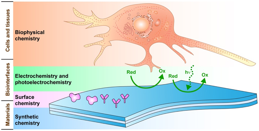
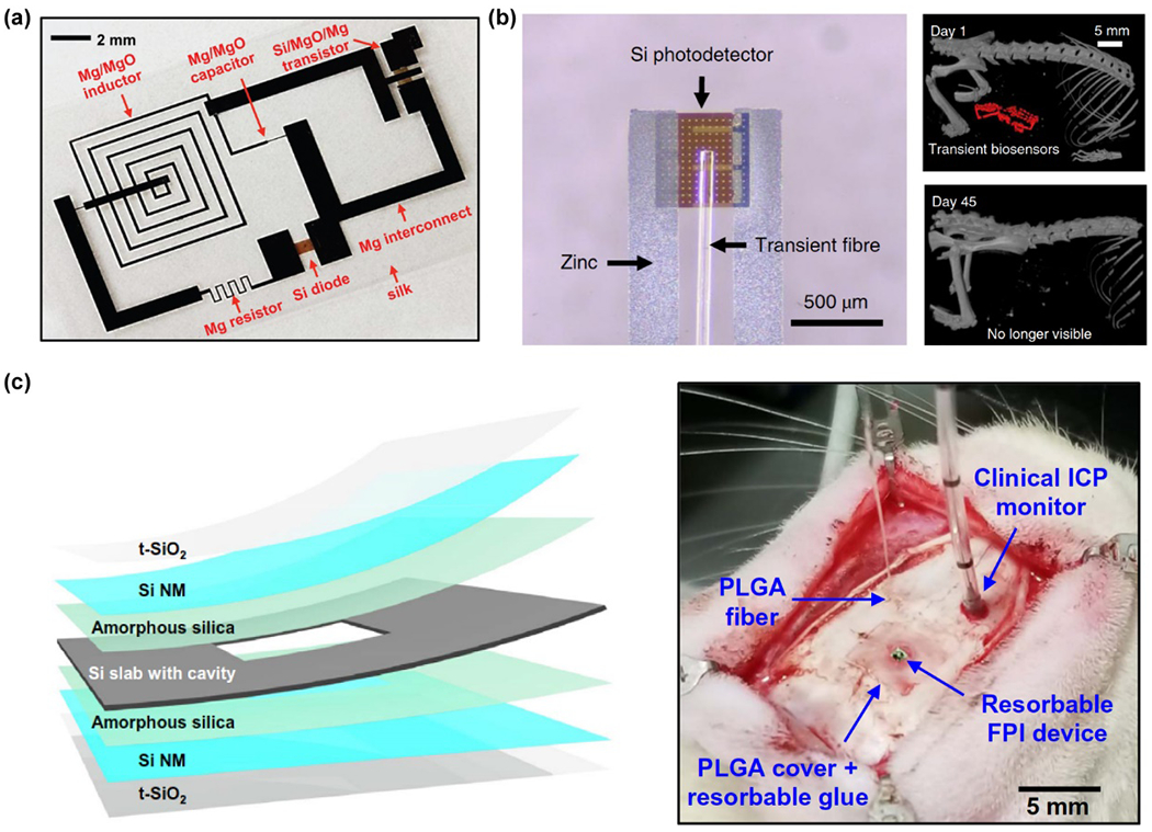
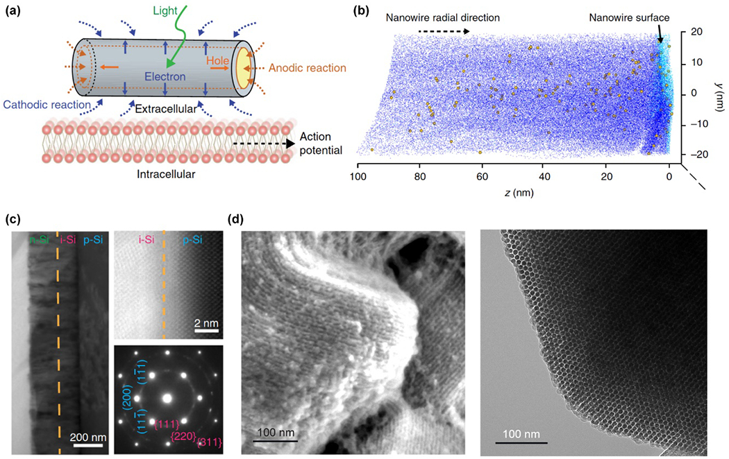
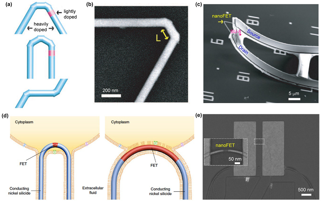
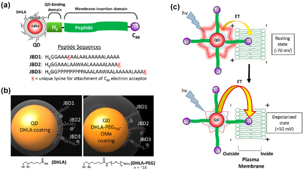
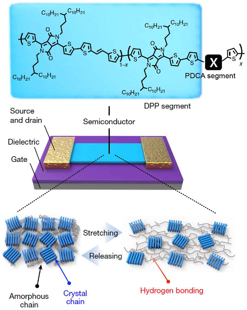
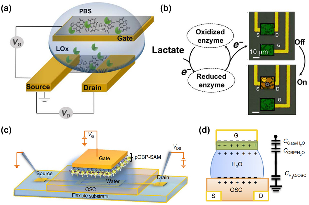
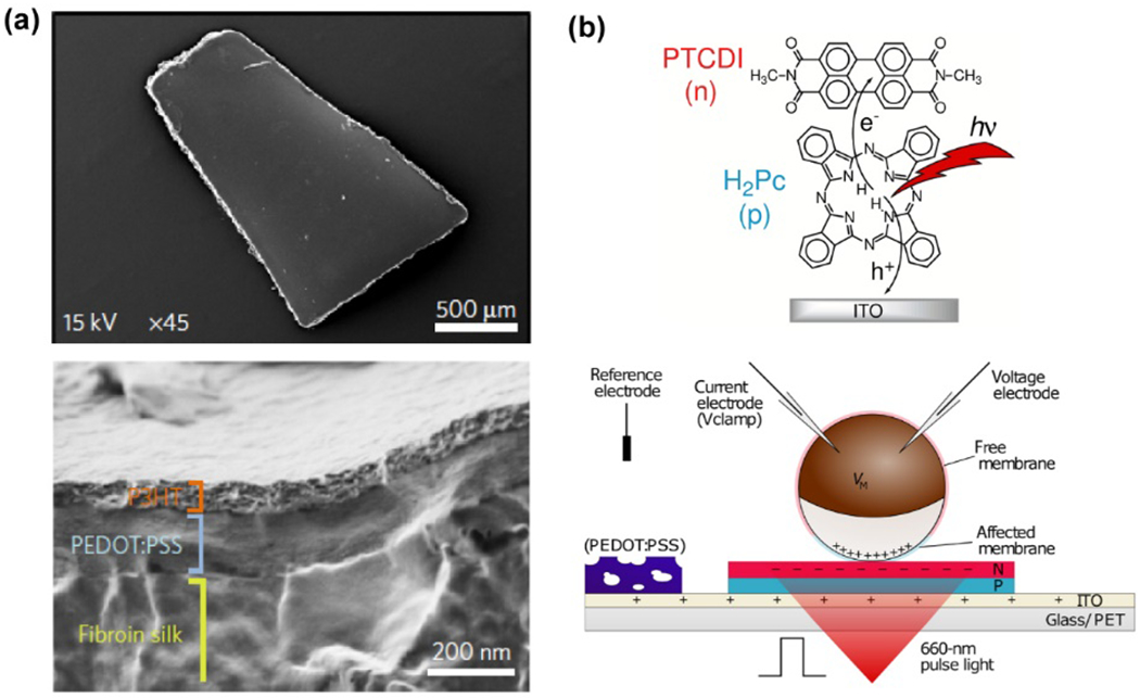
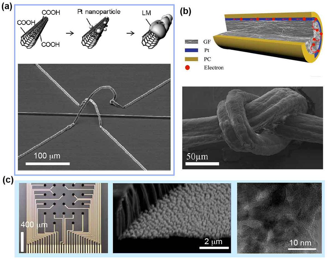
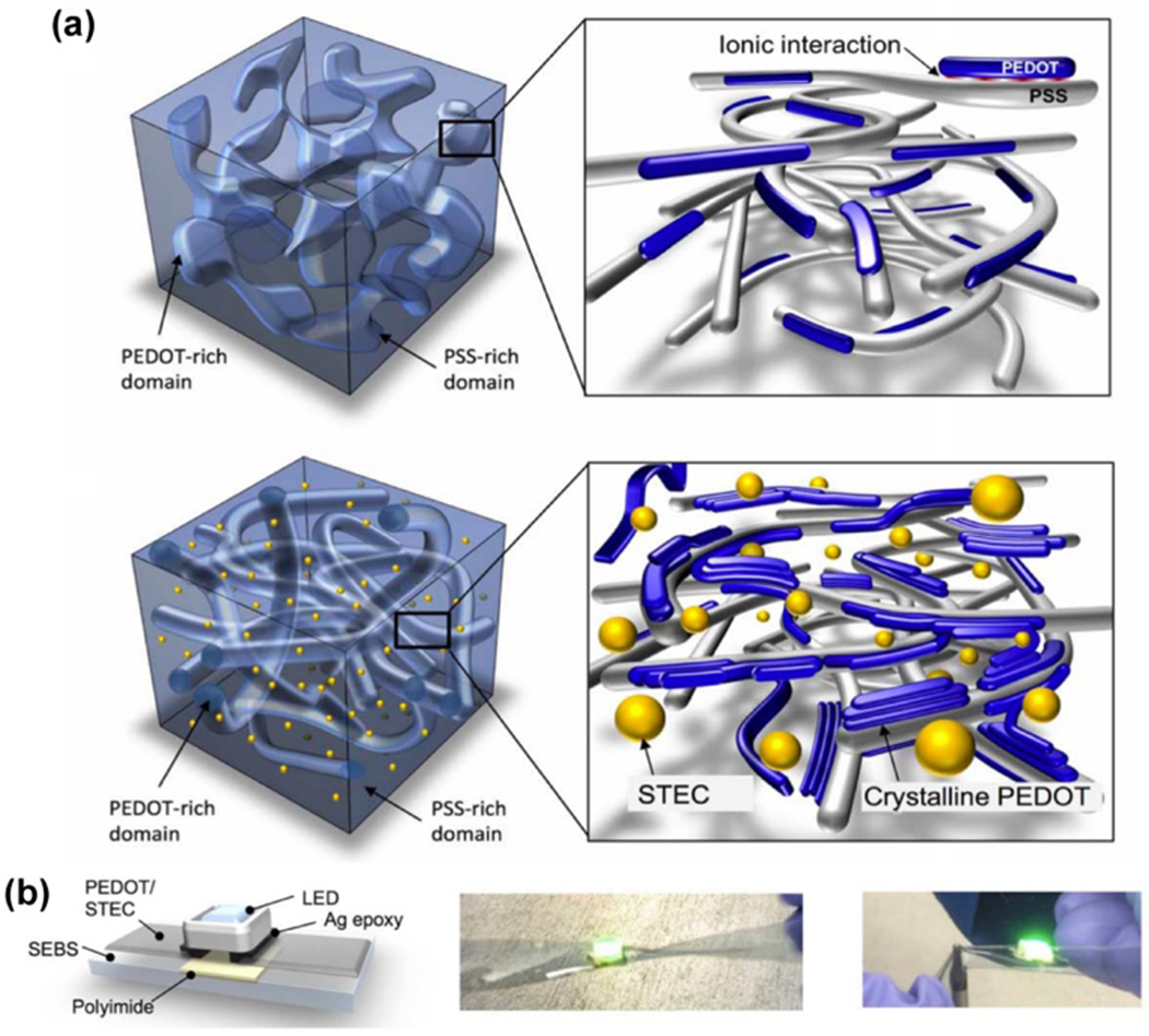
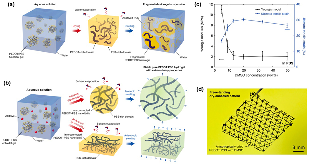
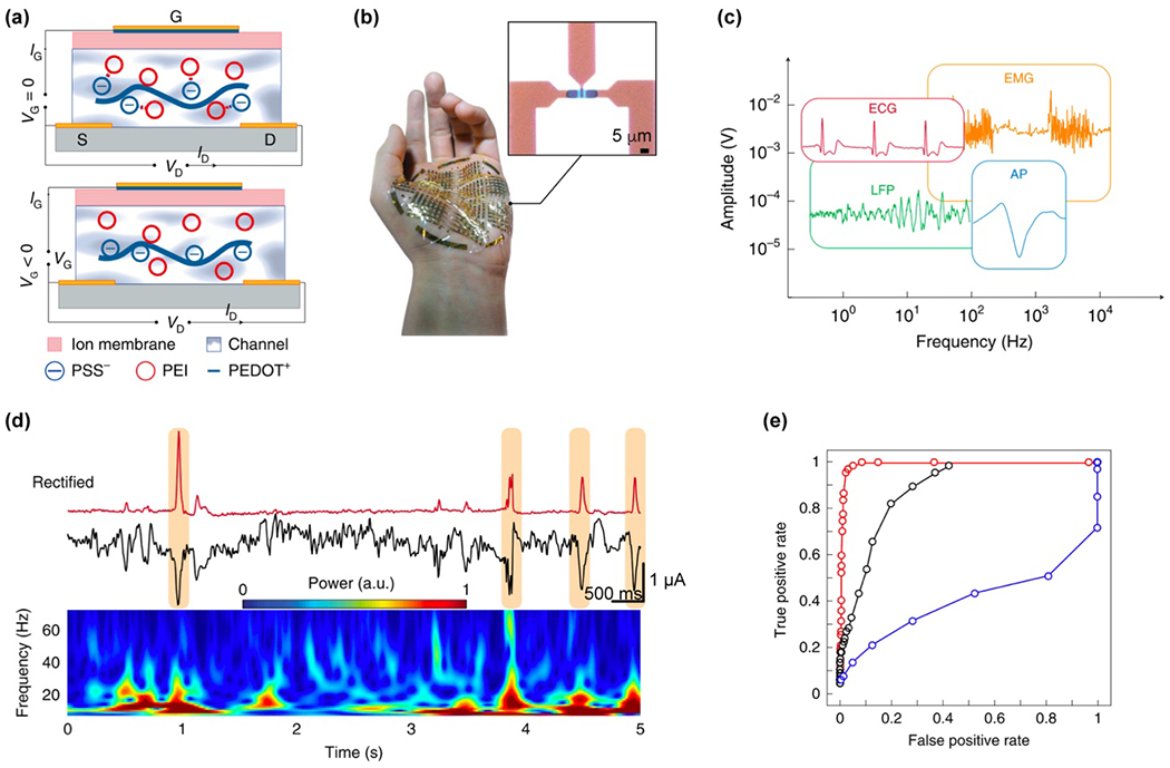
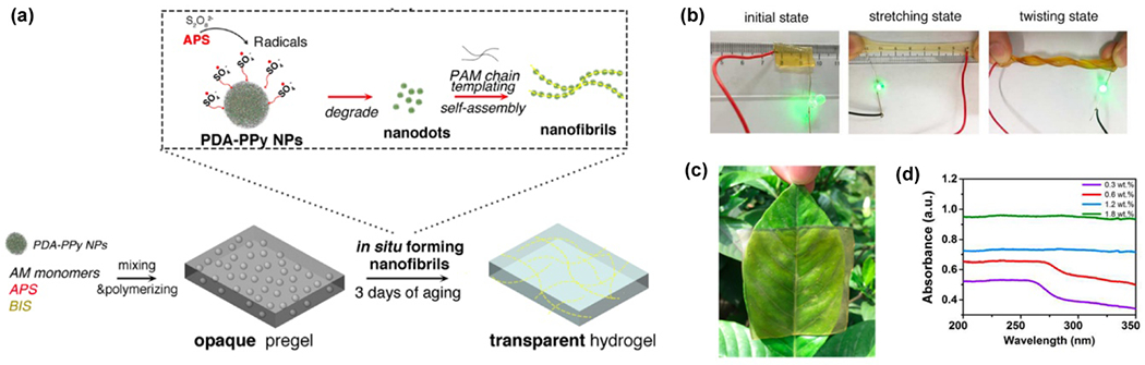
Research in bioelectronics is highly interdisciplinary, with many new developments being based on techniques from across the physical and life sciences. Advances in our understanding of the fundamental chemistry underlying the materials used in bioelectronic applications have been a crucial component of many recent discoveries. In this review, we highlight ways in which a chemistry-oriented perspective may facilitate novel and deep insights into both the fundamental scientific understanding and the design of materials, which can in turn tune the functionality and biocompatibility of bioelectronic devices. We provide an in-depth examination of several developments in the field, organized by the chemical properties of the materials. We conclude by surveying how some of the latest major topics of chemical research may be further integrated with bioelectronics.


Conflict of interest statement

Conflicts of interest: The authors declare no conflicts of interest.

Figures

Figure 1.
Figure 1.
Chemistry aspects of bioelectronics.
Figure 2.
Figure 2.
Bioelectronics and bioelectrical studies span a range of length and time scales. Awareness of chemistry and physics at all applicable levels is necessary to devise appropriate synthetic and analytical methods for the study of biointerfaces.
Figure 3.
Figure 3.
Signal transduction mechanisms in bioelectrical interfaces can vary depending on the material design and chemistry. Top: Metal-based electrodes can be used for recording or injection of capacitive, faradaic, and biocatalytic currents. Free-standing metallic nanostructures allow used for plasmonic heating. Additionally, metallic structures can be used to facilitate interface interrogation penetrating cellular membranes using electroporation and optoporation. Bottom: Highly sensitive recording of bioelectric signals using field-effect transistor (FET) and organic electrochemical transistors (OECT). Readout of optical signals using photoluminescent materials and photodetectors. Free-standing nanoscale semiconductors allow for wireless injection of currents through photocapacitive, photofaradaic and photocatalytic effects. Micro light-emitting diodes (LED) can be used to deliver optical signals. Semiconductors without electric and radiative energy decay pathways can generate photothermal heating.
Figure 4.
Figure 4.
Si nanowires with various structures and morphologies can be produced from metal-assisted chemical etching methods. (a) SiNWs with ordered grooves, etched from a mixture of hydrofluoric acid/hydrogen peroxide. Reproduced from ref. under the terms of the Creative Commons Attribution License from Springer Nature, copyright 2017. (b) SiNWs spicules formed by wet chemical etching in KOH solutions. Reproduced from ref. with permission from the American Association for the Advancement of Science, copyright 2015.
Figure 5.
Figure 5.
Transient and bioresorbable electronics derived from the degradation of Si and other transient materials. (a) Optical image of circuit design and components of a transient device. Reproduced from ref. with permission from the American Association for the Advancement of Science, copyright 2012. (b) Left: photograph of a SiNM-based bioresorbable spectrometer. Right: implanted device can be naturally resorbed after 45 days. Reproduced from ref. with permission from Springer Nature, copyright 2019. (c) Left: a schematic diagram of a SiNM-based bioresorbable sensor designed for the measurements of intracranial pressure (ICP) and temperature (ICT). Right: photograph of the bioresorbable sensor implanted in the intracranial space of a rat. Reproduced from ref. with permission from the American Association for the Advancement of Science, copyright 2019.
Figure 6.
Figure 6.
Si nanostructures used in the photo stimulation of cells. (a) A schematic diagram shows coaxial p-type/intrinsic/n-type (p-i-n) SiNWs for photoelectrochemical extracellular modulation of DRG neuron membrane potential. (b) Atom probe tomography shows the presence of diffused Au (yellow balls) on the sidewalls of p-i-n SiNWs (Si atoms: dark blur; O atoms: light blue). (a) and (b) Reproduced from ref. with permission from Springer Nature, copyright 2018. (c) Cross-section TEM image (left), scanning TEM (STEM) image (upper right) and the diffraction pattern of a p-i-n Si membrane nanostructure applied for the photostimulation of brain cortex and behavior control. Reproduced from ref. with permission from Springer Nature, copyright 2018. (d) Left: SEM image of nanostructures of replica Si from hexagonal mesoporous silica SBA-15, which were applied in the elicitation of action potential by photothermal effect. Right: TEM image shows the hexagonal packing of a Si nanowire. Reproduced from ref. with permission from Springer Nature, copyright 2016.
Figure 7.
Figure 7.
Si-based nanoFET for intracellular recordings. (a) A schematic diagram of the nano-sized FET region, which was introduced by dopant modulation on kinked nanowires. (b) A SEM image of a kinked Si nanowire. (c) NanoFET on an SU-8 microribbon support. (a) – (c) Reproduced from ref. with permission from the American Association for the Advancement of Science, copyright 2010. (d) A schematic diagram of probe internalization and intracellular recording by short channel nanoFETs. (e) SEM image of a U-shape nanoFET with atomically sharp nickel silicide interfaces. (d) and (e) Reproduced from ref. with permission from Springer Nature, copyright 2019.
Figure 8.
Figure 8.
QD applied for bioelectronic voltage sensing in neural membranes. (a) A schematic diagram and (b) molecular models for the design of the QD (electron donor) – peptide-fullerene (electron acceptor) bioconjugated system. (c) A schematic diagram for the fluorescence change introduced by membrane depolarization process. The electrons transfer from the photoexcited QD donor to the fullerene acceptor when the plasma membrane is depolarized, giving rise to the quenching of PL. Reproduced from ref. with permission from the American Chemical Society, copyright 2017.
Figure 9.
Figure 9.
Intrinsically stretchable and healable polymers for fabricating stretchable organic thin-film field effect transistors (OTFTs). 2,6-pyridine dicarboxamide (PDCA) conjugation breaking spacers are integrated with the 3,6-di(thiophen-2-yl)-2,5-dihydropyrrolo[3,4-c]pyrrole-1,4-dione (DPP) semiconductor polymer. The polymer contains crystalline domains (blue) and amorphous polymer chains, where dynamic hydrogen bonds can break and reform. Reproduced from ref. with permission from Springer Nature, copyright 2016.
Figure 10.
Figure 10.
Surface modification of organic transistors for bioelectronic sensing. (a) A schematic diagram of the enzyme biofunctionalization on OECTs devices. (b) LOx enzyme immobilized on the gate electrode of transistors can enhance the sensing selectivity. (a) and (b) Reproduced from ref. with permission from the American Association for the Advancement of Science, copyright 2018. (c) A schematic diagram and (d) working mechanism of a capacitively coupled p-type organic FET with pOBPs as ligands. (c) and (d) Reproduced from ref. under the terms of the Creative Commons Attribution License from Springer Nature, copyright 2015.
Figure 11.
Figure 11.
Organic semiconductors used for optical modulation of cells and tissues. (a) SEM images of photosensitive organic prosthetic implants composed of active P3HT layer, conductive PEDOT:PSS layer, and silk fibroin substrate. Reproduced from ref. with permission from Springer Nature, copyright 2017. (b) A schematic diagram of the organic electrolytic photocapacitors based on H2Pc / PTCDI junction for the X. laevis oocyte photoexcitation. Reproduced from ref. with permission from the American Association for the Advancement of Science, copyright 2019.
Figure 12.
Figure 12.
Pt nanostructures used for bioelectronics. (a) Top: A schematic diagram shows Pt nanoparticles as interface materials in the preparation of carbon nanotube/liquid metal (LM) composite. Bottom: SEM image of a 3D structure of printed Pt/CNTs/liquid metal composites. Reproduced from ref. with permission from the American Chemical Society, copyright 2019. (b) Top: the structure of a Pt coated graphene fiber (GF) with an as yet unrivalled charge injection capacity of ~10 mC⋅cm−2. Graphene, as current collector, improved the charge injection capacity of the system via a strong synergistic effect. Bottom: SEM image of a tied knot shows the flexibility of the graphene microfibers. Reproduced from ref. with permission from Wiley, copyright 2019. (c) Optical image (left), cross-section SEM image (middle), and high-resolution TEM image (right) of the porous Pt nanorods obtained from dissolution Ag from a co-sputtered PtAg alloy. Reproduced from ref. with permission from the American Chemical Society, copyright 2019.
Figure 13.
Figure 13.
Au-based nanostructures used for bioelectronics. (a) SEM images of rat hippocampal cells cultured on Au mushroom microelectrodes. Reproduced from ref. under terms of the Creative Commons Attribution License from Frontiers, copyright 2011. (b) Top: SEM image and backscattered electron (BSE) image (inset) of Au–Ag nanocomposites. Bottom: haematoxylin & eosin (H&E) staining of Ag–Au nanowires implanted cardiac muscles shows little fibrotic reaction and inflammatory response. Reproduced from ref. with permission from Springer Nature, copyright 2018. (c) Top: A schematic diagram of the ultrasoft Au-deposited parylene–polyurethane nanomesh (left). This ultrasoft electronics can be used for mapping the electrophysiological dynamics during cardiomyocytes beating (right). Bottom: An optical image of the ultrasoft nanomesh. Reproduced from ref. with permission from Springer Nature, copyright 2018.
Figure 14.
Figure 14.
Carbon microfiber used for intracellular electrochemical detection. (a) SEM of an insulated carbon microelectrode with nanoscale tip. Reproduced from ref. with permission from the American Chemical Society, copyright 2020. (b) A schematic diagram shows single-cell intracellular measurements of vesicles and synaptic activities using a carbon-fiber microelectrode. (c) On a carbon electrode, vesicles rupture and expel contents, for example norepinephrine (i), epinephrine (ii), octopamine (iii) or dopamine (iv). The elicited oxidation currents can be electrochemically detected by the carbon microelectrode. (b) and (c) Adapted from ref. with permission from Springer Nature, copyright 2017.
Figure 15.
Figure 15.
Graphene-based bioelectronics. (a) A schematic diagram of the serpentine Au mesh/graphene-based diabetes patch with sweat-control, sensing and therapy components. (b) Optical images of the compressed (top) and stretched (bottom) diabetes patches. (a) and (b) Reproduced from ref. with permission from Springer Nature, copyright 2016. (c) A schematic diagram shows the fabrication steps to obtain soft graphene contact lens on Parylene C. (d) Top: infrared fundus photo of a monkey eye taken during multifocal electroretinography (ERG) recording with a soft graphene contact lens (or GRACE device). Bottom: The response density plot of ERG signals in associated regions. (c) and (d) Reproduced from ref. under the terms of the Creative Commons Attribution License from Springer Nature, copyright 2018.
Figure 16.
Figure 16.
Hierarchical carbon fiber-based bioelectronics. (a) A schematic diagram shows the hierarchical helical bundles of muscle. (b) Top: TEM image of a multi-walled CNT, the building block for a CNT-based hierarchical helical bundle. Middle: SEM image of a primary CNT-based fibre. Bottom: SEM image of assembled hierarchical helical CNT bundles. (c) Left: a schematic diagram shows the CNT helical fibre bundles can be injected into blood vessel for in vivo monitoring. Right: photograph of the skin surface of a cat after injection with a CNT-based multiply sensing fibre. (a) − (c) Reproduced from ref. with permission from Springer Nature, copyright 2019.
Figure 17.
Figure 17.
STEC-enabled PEDOT:PSS bioelectronics. (a) Schematic representations of PEDOT:PSS domains in a pristine polymer (top) and with an addition (bottom) of stretchability and electrical conductivity enhancer. (b) Left: schematic representation of LED device with interconnects made of PEDOT/STEC. Middle: photograph shows high LED brightness when the device is stretched and twisted. Right: photograph shows high LED brightness when the device is poked with a sharp object. (a) and (b) Reproduced from ref. with permission from the American Association for the Advancement of Science, copyright 2017.
Figure 18.
Figure 18.
Pure PEDOT:PSS hydrogel and freestanding structure. (a) Schematic representation of PEDOT:PSS domains aggregation during water evaporation. (b) Schematic representation of fibril domain morphology in PEDOT:PSS hydrogel dried with DMSO as an additive. (c) DMSO dependent Young’s moduli and ultimate tensile strains in the pure PEDOT:PSS gels. (d) Free-standing PEDOT:PSS pattern fabricated using inkjet printing. (a) − (d) Reproduced from ref. under the terms of the Creative Commons Attribution License from Springer Nature, copyright 2019.
Figure 19.
Figure 19.
e-IGT for bioelectronics. (a) Schematic illustration of e-IGT device operation. Protonation of PEI+ under negative gate potential releases PSS- which upon binding to PEDOT reinstitutes its conductivity. (b) Photograph showing conformance of the ultra-thin e-IGT based device to the human hand. Inset shows the microphotograph of an individual junction. (c) Traces of sample signals recorded with e-IGT-based devices spanning through amplitude and frequency ranges. (d) Output of nonlinear rectifier made of IGT-based circuit. Top: marked spikes show epileptic discharges. Bottom: Power spectrogram of the recording. (e) Operating curves showing improved detection performance of nonlinear amplifier (red) over bandpass filter (black) and amplitude (blue) thresholding. (a) – (e) Reproduced from ref. with permission from Springer Nature, copyright 2020.
Figure 20.
Figure 20.
PDA-PPy hydrogels. (a) Schematic representation of in situ transformation of PDA-PPy nanoparticles into transparent fibrils. (b) Demonstration of the electrical conductivity of the hydrogel (6 wt. %) under stretching and twisting. (c) Photography of transparent hydrogel on a leaf. (d) UV-vis absorption spectra of hydrogels prepared with different PDA-PPy concentration. (a) – (d) Reproduced from ref. with permission from the American Chemical Society, copyright 2018.
Figure 21.
Figure 21.
Structured PPy for mechanotransduction. (a) Schematic representation of structure switching in PPy array directing development of Mesenchymal stem cells. (b) SEM images of PPy array at the two redox states showing nanotube and nanotip geometry. Mechanotransduction effects on (c) distribution of actin filaments (pseudocoloured heat maps, scale bar 10 um), (d) cell area, and (e) nuclear translocation. (a) – (e) Reproduced from ref. with permission from the American Chemical Society, copyright 2017.
Figure 22.
Figure 22.
Genetically targeted chemical assembly of polymers. (a) A schematic diagram shows specific synthesis of functional polymer on membranes of genetically modified neurons. (b) Scheme of Apex2-catalyzed polymerization reaction initiated by oxidation of aniline dimer. Chemical species participating in a reaction are as follows: (1) aniline dimer, (2) aniline dimer radical cations, (3) aniline monomer, (4) aniline trimer radical cations, and (5) polyaniline (PANI). Patch clamp measurements of membrane capacitance and current potential spikes from neurons show that modification with conductive PANI increases transmembrane capacitance and decreases spike number (c) while modification with insulating poly(3,3’-diaminobenzidine) (PDAB) inversely reduces the capacitance and increases spike number. (a) – (d) Reproduced from ref. with permission from the American Association for the Advancement of Science, copyright 2020.
Figure 23.
Figure 23.
A minimal mechanical model of a cell. Top: schematic of an entire mammalian cell, with the nucleus shown in blue and the cytosol in grey. Green arrows indicate locations, orientations, and relative magnitudes of traction stresses. Lower left: mechanical components around the cell nucleus. The actin cytoskeleton is linked to the nucleoskeleton through the LINC complex. Within the nucleus, YAP/TAZ are effectors of Hippo signaling, which ultimately governs cell spreading and proliferation. Lower right: mechanical components at the cell edge. Traction stresses are transmitted from the cytoskeleton to the substrate through focal adhesions. The RhoA pathway is especially active at focal adhesions and modulates cell contractility by affecting the activity of myosin light chain kinase, MLCK. Piezo channels are both mechanically and electrically active, and therefore are integral parts of electromechanical coupling.
Figure 24.
Figure 24.
Photoisomerization-triggered neuromodulation. (a) Top: snapshots from MD simulations of a membrane-bound photoswitch, Ziapin2, in trans- and cis-conformations. Bottom: current-clamp traces from neurons incubated with Ziapin2. Illumination period is indicated with cyan shading. Reproduced from Ref. with permission from Springer Nature, copyright 2020. (b) Schematic of how photoisomerization can induce appreciable mechanical deformations in a material, useful for applications such as switchable adhesions and robotic actuators. Reproduced from Ref. with permission from Wiley, copyright 2019.
Figure 25.
Figure 25.
Schematic of LOVpep-based optogenetic dimerization. Illumination exposes the PDZ-binding domain of LOV2, thereby causing dimerization with PDZ domain proteins. Reproduced from Ref. with permission from Springer Nature, copyright 2012.
Figure 26.
Figure 26.
Schematic of remotely controlled chemomagnetic neuromodulation. (a) Magnetically responsive liposomes release chemical payloads upon magnetic heating and stimulate the receptors. (b) The liposomes can be injected into the ventral tegmental area, a region typically used for motivated behavior, reward and depression studies. (a) and (b) Reproduced from Ref. with permission from Springer Nature, copyright 2019.
Figure 27.
Figure 27.
Biomimetic targets and designs. (a) Schematic showing conformation of geometrically adaptable heart valve when implanted in a juvenile sheep, in the unextended conformation. (b) Schematic showing conformation of geometrically adaptable heart valve when implanted in mature sheep. In this case, the needed pulmonary valve dimensions are 1.8x larger than the juvenile case. (a) and (b) Reproduced from Ref. with permission from the American Association for the Advancement of Science, copyright 2020. (c) Electric eel-mimicking hydrogel array. Red gel is high concentration NaCl, blue gel is low concentration NaCl, green gel is cation-selective, and yellow gel is anion-selective. Reproduced from Ref. with permission from Springer Nature, copyright 2017.
Figure 28.
Figure 28.
Chemical considerations in electron transfer and electrode selection for bioelectrocatalysis. (a) Direct electron transfer (DET) and mediated electron transfer (MET) schemes. DET is shown both wired and unwired. Reproduced from Ref. with permission from Springer Nature, copyright 2020. (b) A view of a protein chimera nanowire used for wiring in a synthetic redox film. Reproduced from Ref. with permission from Springer Nature, copyright 2016. (c) Diagram of how enhanced wettability of electrode surface can improve the electrochemical performance of a catalyst. Reproduced from Ref. with permission from the Wiley, copyright 2014.
Figure 29.
Figure 29.
Nanofibrillar cellulose and lignin form good substrates for bioelectronic supercapacitors. (a) Photograph of nanocellulose fibrillar paper and molecular structures for different types of nanocellulose fibers. (b) SEM image of PPy-nanocellulose fiber composite material. (a) and (b) Reproduced from Ref. with permission from the American Chemical Society, copyright 2015. (c) SEM image of lignin-derived carbon nanofiber mat. (d) 3D visualization of lignin-derived carbon nanofiber maps obtained from computed tomography. (c) and (d) Reproduced from Ref. under the terms of the Creative Commons Attribution License from the Royal Society of Chemistry, copyright 2019.

Similar articles

Cited by

References

    1. Zhang A and Lieber CM, Chemical Reviews, 2016, 116, 215–257. - PMC - PubMed
    1. Chortos A, Liu J and Bao Z, Nature Materials, 2016, 15, 937–950. - PubMed
    1. Jonsson A, Inal S, Uguz I, Williamson AJ, Kergoat L, Rivnay J, Khodagholy D, Berggren M, Bernard C, Malliaras GG and Simon DT, Proceedings of the National Academy of Sciences, 2016, 113, 9440. - PMC - PubMed
    1. Mickle AD, Won SM, Noh KN, Yoon J, Meacham KW, Xue Y, McIlvried LA, Copits BA, Samineni VK, Crawford KE, Kim DH, Srivastava P, Kim BH, Min S, Shiuan Y, Yun Y, Payne MA, Zhang J, Jang H, Li Y, Lai HH, Huang Y, Park SI, Gereau RW and Rogers JA, Nature, 2019, 565, 361–365. - PMC - PubMed
    1. Cingolani E, Goldhaber JI and Marbán E, Nature Reviews Cardiology, 2018, 15, 139–150. - PMC - PubMed