

Review
doi: 10.3390/nano10071392.
Current Trends in Nanomaterials for Metal Oxide-Based Conductometric Gas Sensors: Advantages and Limitations. Part 1: 1D and 2D Nanostructures
Affiliations
- PMID: 32708967
- PMCID: PMC7407990
- DOI: 10.3390/nano10071392
Item in Clipboard
Review
Current Trends in Nanomaterials for Metal Oxide-Based Conductometric Gas Sensors: Advantages and Limitations. Part 1: 1D and 2D Nanostructures
Nanomaterials (Basel).
.
Abstract
This article discusses the main uses of 1D and 2D nanomaterials in the development of conductometric gas sensors based on metal oxides. It is shown that, along with the advantages of these materials, which can improve the parameters of gas sensors, there are a number of disadvantages that significantly limit their use in the development of devices designed for the sensor market.
Keywords: fabrication; improvement; individual 1D structures; nanobelts; nanosheets; nanowire array; nanowires; stability; synthesis.
Conflict of interest statement
The author declare no conflict of interest.
Figures
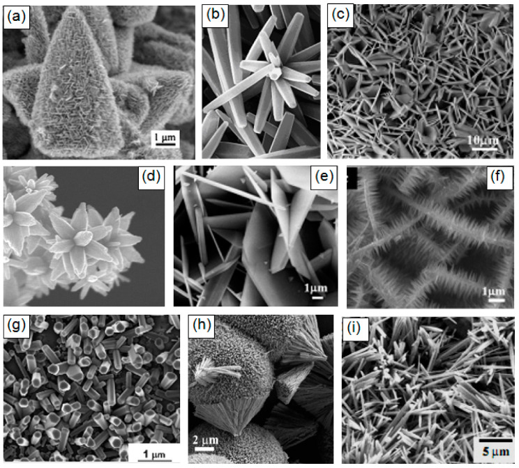
SEM images of ZnO and Cu2O nanostructures synthesized by different methods. Reproduced with permission from (a) Lu et al. [87]. Copyright 2008: Willey-VCH Verlag GmbH; (b) Li et al. [88]. Copyright 2008: Elsevier; (c,e,f) Xu et al. [89]. Copyright 2007: ACS; (d) Sepulveda-Guzman et al. [90]. Copyright 2009: Elsevier; (g) Krunks et al. [91]. Copyright 2006: Elsevier; (h) Orel et al. [92]. Copyright 2007: ACS; (i) Dev et al. [93]. Copyright 2006: Institute of Physics.
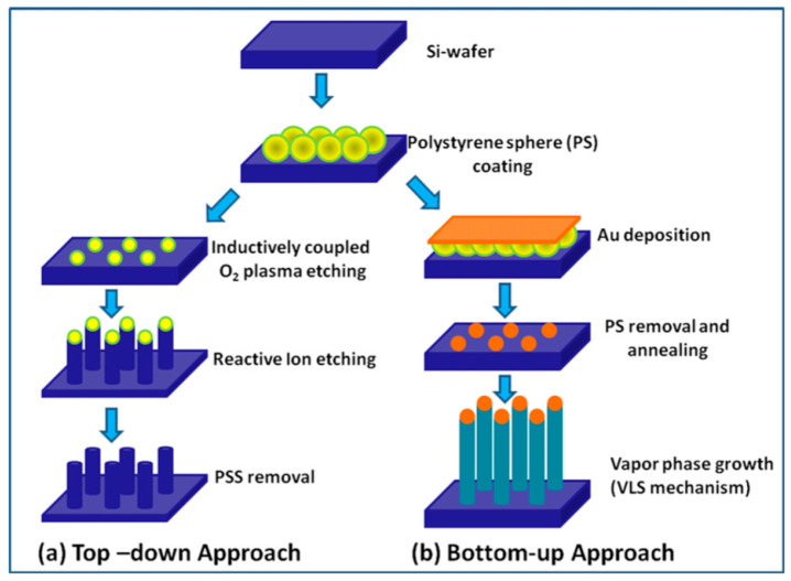
Schematic presentation of general steps involved in the fabrication of nanowires (NWs) using (a) top-down and (b) bottom-up approaches. Reproduced with permission from Ramgir et al. [130]. Copyright 2013: Elsevier.
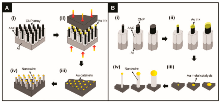
The schematic diagrams depict (A) the entire procedure, which includes (i) the fabrication of the carbon nanopost (CNP) stamps, (ii) the contact-printing of the Au ink, (iii) the preparation of the Au metallic catalysts, and (iv) the growth of the semiconductor NWs over the contact-printed Au catalysts via the vapor-liquid-solid (VLS) process; and (B) the conceptual model of the size-controlled fabrication of semiconductor NWs via the contact-printing process using the CNP stamps with different tip diameters: (i) Different-sized CNP tips, (ii) Au ink that was loaded onto the CNP tips, (iii) contact-printed Au catalysts from the CNP tips, and (iv) NWs grown over the size-controlled Au catalysts. The variation of the CNP diameter, which was used as the stamps for contact-printing of the Au catalysts, directly controls the diameter of the NWs that are grown over the printed Au particles. Reproduced with permission from Lee et al. [135]. Copyright 2010: American Chemical Society.
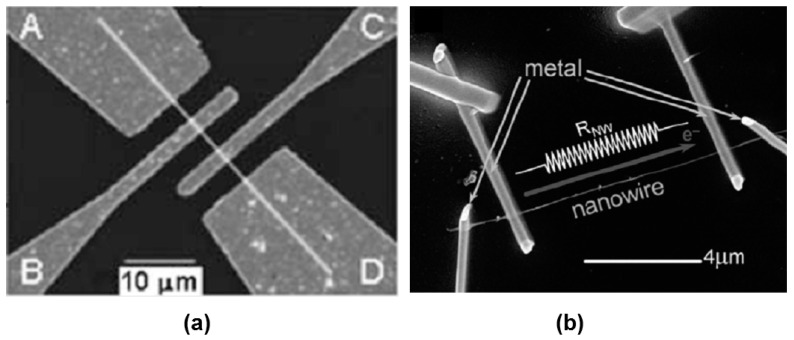
SEM images of gas sensors based on single metal oxide nanobelts and nanowires. (a) Reprinted with permission from Fields et al. [148]. Copyright 2006: American Institute of Physics. (b) Reproduced with permission from Hernandez-Ramirez et al. [149]. Copyright 2009: Royal Society of Chemistry.
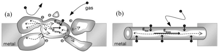
Diagrams illustrating the difference in gas sensing effects in (a) the polycrystalline material and (b) individual nanowires: One can see that any intergrain necks or boundaries are absent in 1D-based sensors. Moreover, Ebar and Ebias fields are always orthogonal and independent. Reproduced with permission from Hernandez-Ramirez et al. [149]. Copyright 2009: Royal Society of Chemistry.
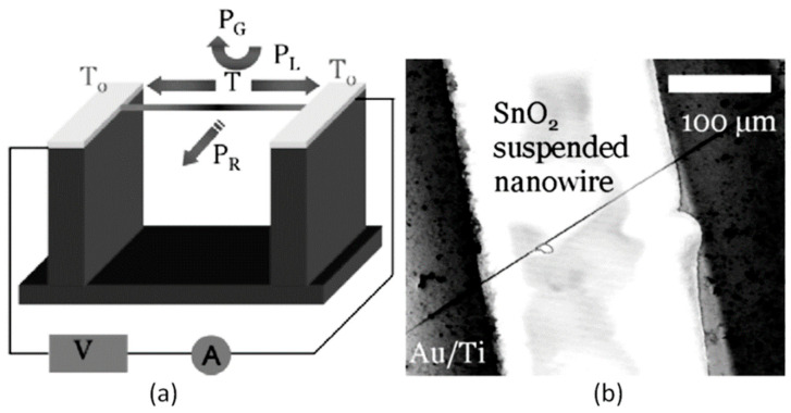
(a) The sensor setup and principal thermal losses in the suspended nanowire heated by the Joule heat: PL-losses to the contacts, PG- losses to the ambient gas, and PR -radiation losses; (b) SEM image of the suspended SnO2 chemiresistor. Reproduced with permission from Strelcov et al. [168]. Copyright 2009: American Institute of Physics.
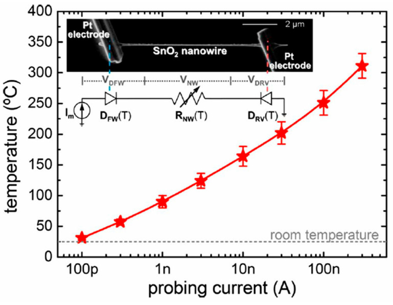
Estimated temperature of the devices at different Im. (rnw~35 nm) (inset) SEM image of a SnO2 nanowire connected to two Pt microelectrodes fabricated with a focused ion beam. The equivalent circuit of this structure corresponds to two back-to-back diodes in a series with the nanowire resistance. These three components dissipate electrical power and contribute to the self-heating of the device. Reproduced with permission from Prades et al. [169]. Copyright 2008: American Institute of Physics.
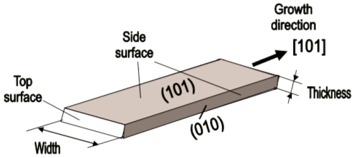
Schematic diagram of the geometric configuration of SnO2 nanobelts. Reproduced with permission from Korotcenkov [74]. Copyright 2008: Elsevier.
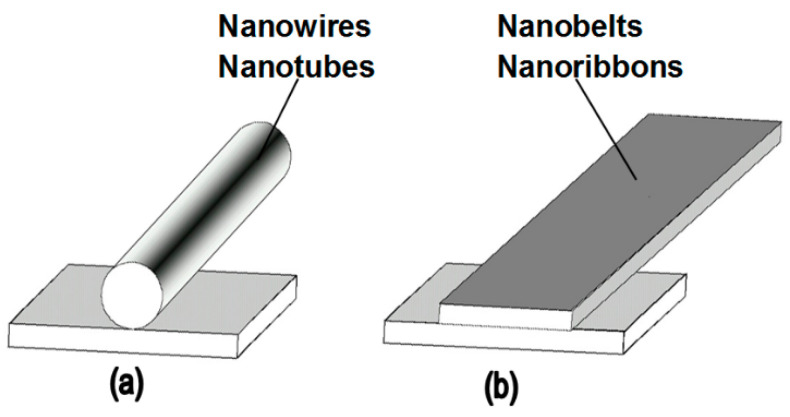
Position of (a) nanowires or nanotubes and (b) nanobelts on the contact pad. Reproduced with permission from Korotcenkov [74]. Copyright 2008: Elsevier.
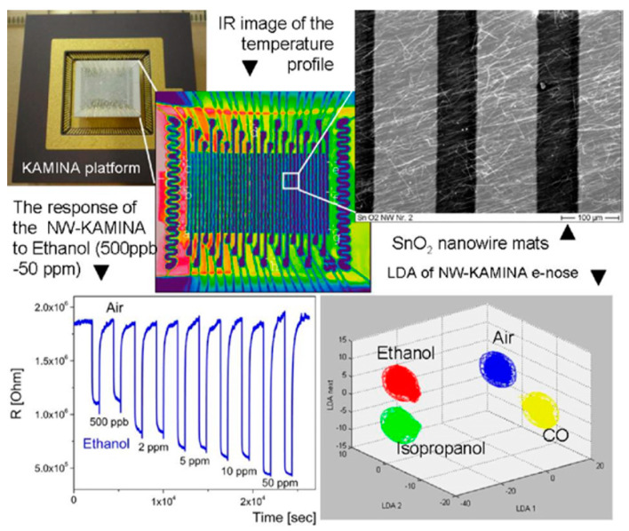
A demonstration of the KAMINA e-nose system performance with SnO2 nanowires as a sensing media. Reproduced with permission from Sysoev et al. [213]. Copyright 2007: American Chemical Society.
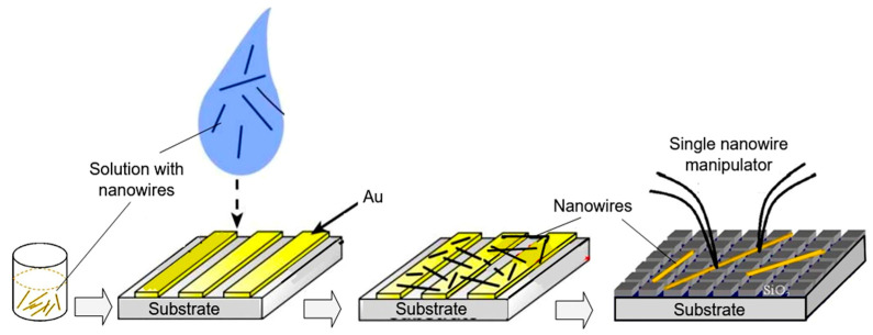
Illustration of the process of transferring 1D structures to the surface of the substrate: Nanowires are removed into a suspension of the solvent. A drop of the nanowire solution is dispersed on a template substrate and evaporated under a vacuum. Finally, nanowires with manipulator tips can be moved from a template substrate to the right place.
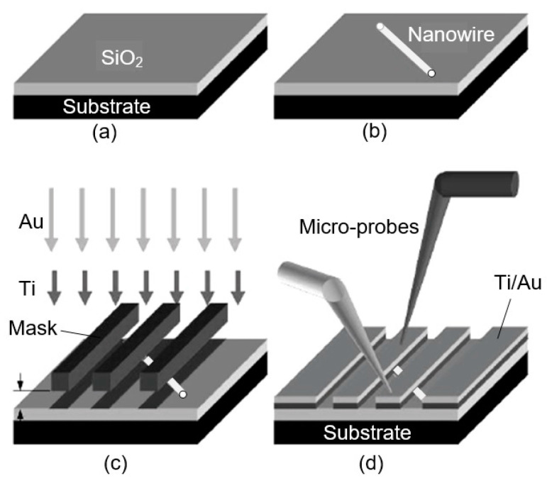
Protocol for a resist-free fabrication of 1D metal oxide nanowire-based chemiresistors and chemFETS: (a) Pristine Si/SiO2 wafer; (b) nanostructures placed on wafer mechanically; (c) shadow masking to determine metal contacts; (d) microprobes can be used to explore transport and sensing properties of the individual nanoresistors. Idea from [234].
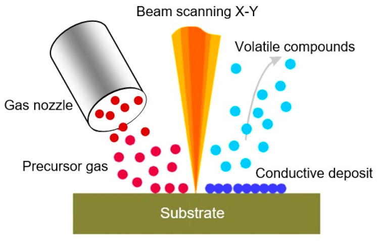
Schematic representation of local deposition, assisted by the focused ion beam (FIB). The gas precursor introduced by the capillary is decomposed by the secondary electrons generated by the interaction of the primary ion beam with the target. Reproduced with permission from Gierak [237]. Copyright 2009: Institute of Physics.
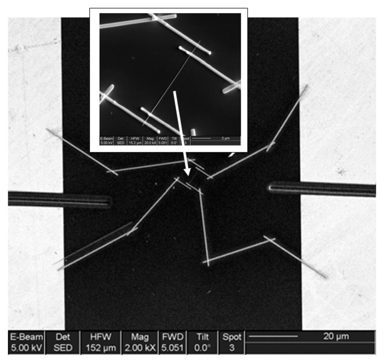
General view of the final device based on the SnO2 individual nanowire (dimensions: L = 11 μm (length) and D = 55 ± 5 nm (diameter)) with Au/Ti/Ni microelectrodes. The position of the contacted NW is indicated by the arrow. Reproduced with permission from Hernandez-Ramirez et al. [159]. Copyright 2007: Elsevier.
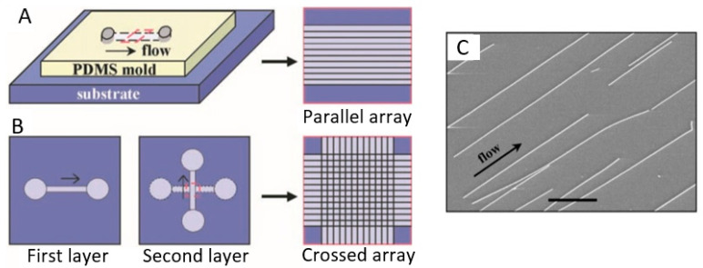
Schematic of fluidic channel structures for flow assembly: (A) A channel formed when the polydimethylsiloxane (PDMS) mold was brought in contact with a flat substrate. The NW assembly was carried out by flowing a NW suspension inside the channel with the controlled flow rate for a set duration. Parallel arrays of NWs are observed in the flow direction on the substrate when the PDMS mold is removed. (B) The multiple crossed NW array can be obtained by changing the flow direction sequentially in a layer-by-layer assembly process. (C) SEM image of the parallel assembly of NW arrays formed using the micro fluidics method. Reproduced with permission from Huang et al. [270]. Copyright 2001: AAAS.
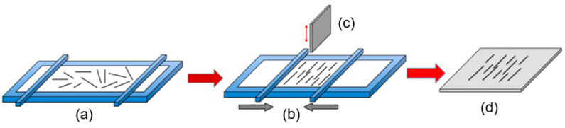
Schematic diagram of the Langmuir-Blodgett technique for NWs alignment. (a) Random nanowires suspended in the Langmuir-Blodgett trough; (b) monolayer compression; (c) wafer being pulled vertically from the suspension in parallel with the lateral motion of the barrier; (d) resulting parallel nanowire array on the substrate.
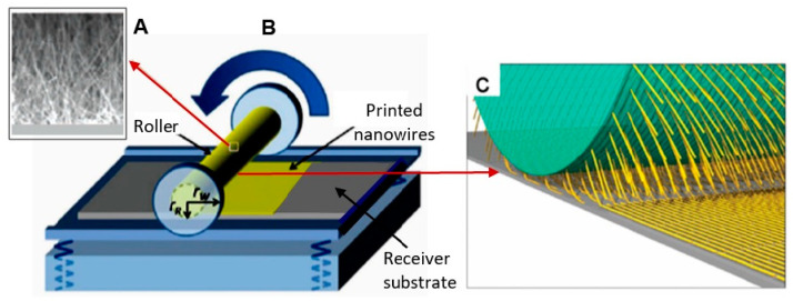
Schematic diagram illustrating the roll printing technique for NWs alignment: (A) SEM image of NWs grown perpendicularly to the surface of the cylindrical substrate; (B) installation for NWs alignment; (C) the mechanism of a nanowire transfer. The NWs are oriented and transferred to the receiving substrate by applying a directional shear force, resulting in the printing of sub-monolayer parallel NW arrays on the receiving substrate. Reproduced with permission from Hu et al. [269]. Copyright 2020: Royal Society of Chemistry.
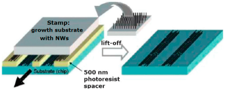
Contact printing of NWs from a growth substrate on a prepatterned substrate. In general, NWs are grown perpendicularly to substrate with a random orientation, but they can be well-aligned by shear forces during the printing process. Reproduced with permission from Javey et al. [271]. Copyright 2007: Royal Society of Chemistry.
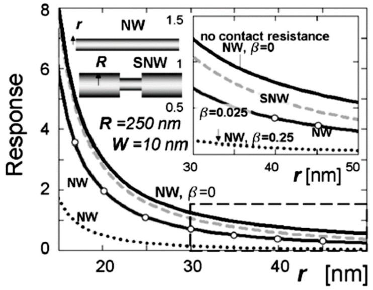
The response of straight and segmented nanowires as a function of their radius at various contact resistances (b = 0, 0.025, 0.25). For segmented nanowires (SNWs), the curve is drawn versus the radius of the smaller segment. The solid curve (top) corresponds to the nanowire with no contact resistance; the dashed curve corresponds to the SNW with thick segments of a 500 nm diameter and b = 0.025; the solid curve marked with circles corresponds to the SNW with b = 0.025; the dotted curve corresponds to the SNW with b = 0.25. The depletion width is ~10 nm at all cases. Reproduced with permission from Dmitriev et al. [274]. Copyright 2007: Institute of Physics.
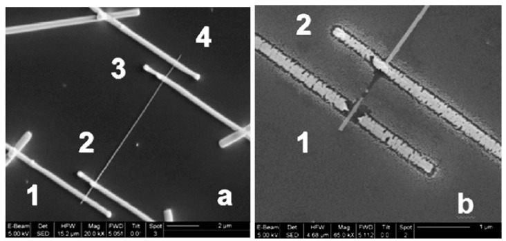
(a) A fabricated FIB four-probes contacted SnO2 nanowire and (b) a detail of the contact after an electrical failure likely caused by the excess of heat dissipation in the contacts. Reproduced with permission from Hernandez-Ramirez et al. [159]. Copyright 2007: Elsevier.
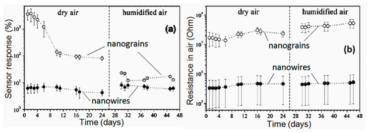
The change of sensing characteristics of the median sensor segment of a SnO2 3D mesoporous nanoparticle (NP) or nanograins (NG) layer and nanowire (NW) mat versus measurement day: (a) Sensitivity or response to 1 ppm of 2-propanol vapors; (b) background resistance in air. Open and filled circles correspond to the NP and NW samples, respectively. Reproduced with permission from Sysoev et al. [129]. Copyright 2009: Elsevier.
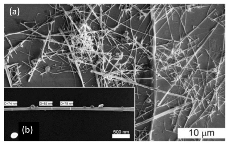
(a) SEM image of SnO2 nanowires after the synthesis using the gas transport method based on the vapor-liquid-solid (VLS) mechanism, and (b) SEM image of a single SnO2 nanowire. Reproduced from Shaposhnik et al. [292]. Published by Beilstein Sci. as open access.
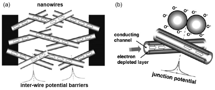
(a) Schematic diagrams for multi-nanowire-based chemical sensors; (b) schematic illustration of the gas sensing mechanism in a network of nanowires. Reproduced with permission from Vomiero et al. [294]. Copyright 2007: American Chemical Society.
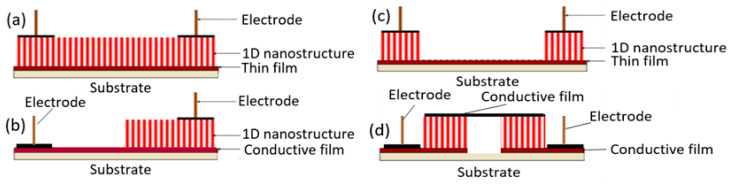
(a–d) Schematic diagrams for a multi-nanowire-based sensor with nanotubes, nanowires, or nanorods oriented in a perpendicular direction.
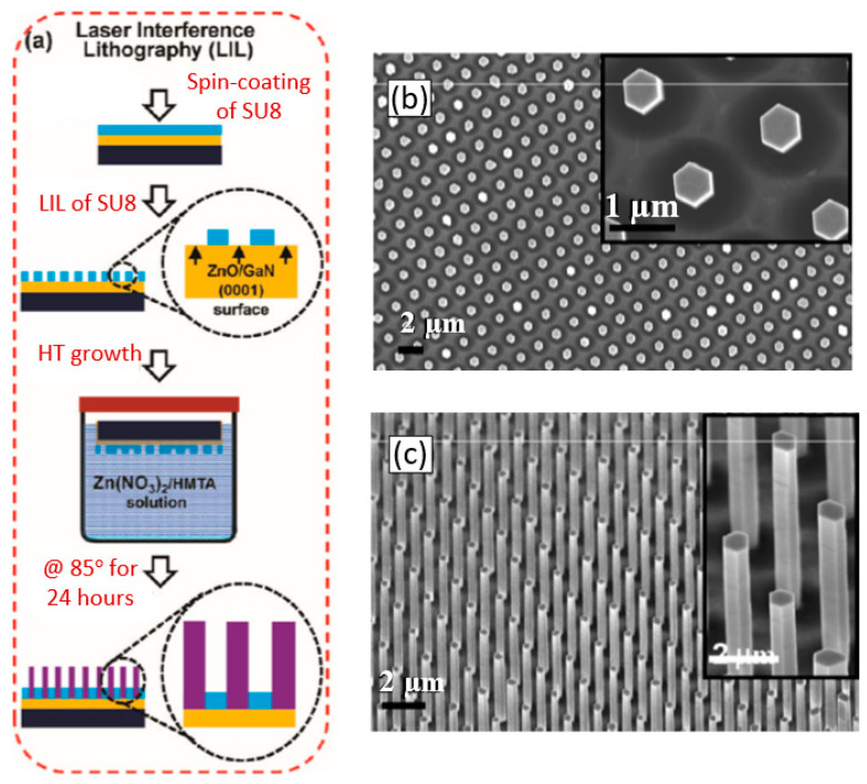
(a) Schematics of the fabrication sequences of vertically aligned ZnO NW arrays using laser interference lithography (LIL); (b) optical image of a 2 in. Si wafer with a SU-8 open-hole pattern over the whole surface area. The iridescence dispersion demonstrates the excellent periodicity over the entire wafer surface. (c) The top-view SEM image of the patterned SU-8 film (thickness of 500 nm). Inset, the top-view SEM image of the patterned SU-8 film at higher magnification. The area encircled by the black dashed line is the exposed surface of the substrate. Reproduced with permission from Wei et al. [302]. Copyright 2010: American Chemical Society.
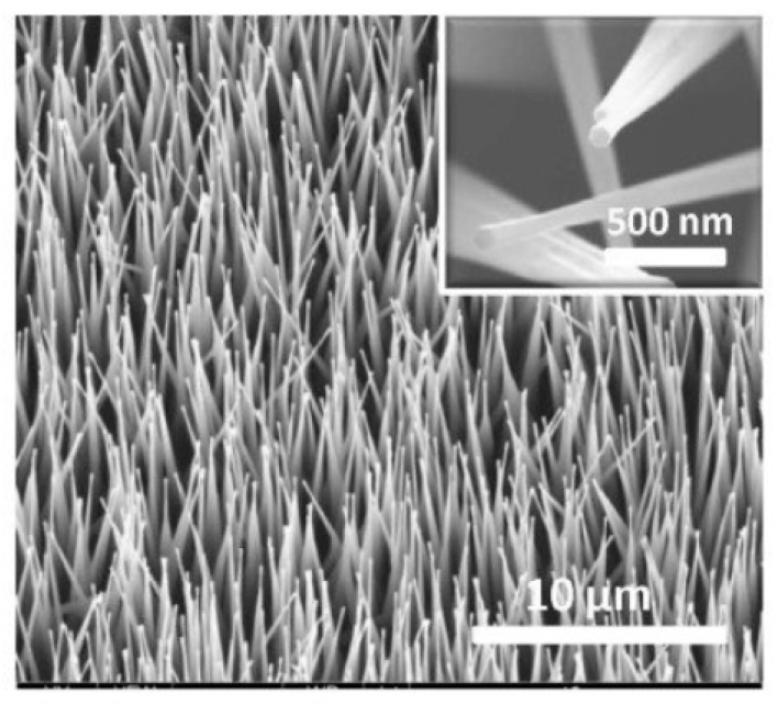
FESEM image (tilted at 15°) of a directly synthesized vertically aligned ZnO nanowire array on a fluorine-doped tin oxide (FTO) substrate. The inset is a higher-magnification image. Reproduced from Lu et al. [306]. Published by Springer as open access.
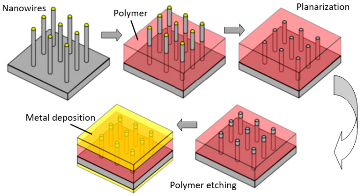
Schematic illustration of the contact forming on the top of vertically grown NWs.
SEM images of Au nanoparticles attached to the tips of the nanowire assembly at different stages of the deposition: (a) 10 min; (b) 1 h; (c) 2 h. Scale bars = 1 µm. Reproduced with permission from Parthangal et al. [309]. Copyright 2007: Cambridge University Press.
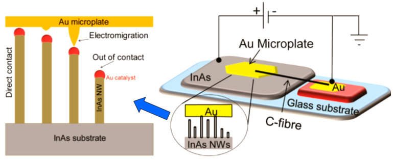
Schematic showing the device configuration of Au microplate/InAs NWs sandwich. Reproduced with permission from Radha et al. [310]. Copyright 2012: American Chemical Society.
(a) Schematic illustration of ZnO-nanowire air bridges over the SiO2/Si substrate. (b) Side- and (d) top-view SEM images clearly show the selective growth of ZnO nanowires on the Ti/Pt electrode. (c) The junction between ZnO nanowires, grown on both electrodes. Reproduced with permission from Ahn et al. [312]. Copyright 2009: Elsevier.
(a) SEM images of ZnO NWs grown on substrates with the Au electrodes (electrode line width × gap distance = 3 × 5 µm); (b) schematic representation of the nanobridge junctions formed and (c) sensor response to the CO gas. Reproduced with permission from Yuon et al. [313]. Copyright 2010: American Chemical Society.
(a,b) Schematic of the bridging NW growth. Reproduced with permission from Huang et al. [219]. Published by Elsevier as open access; (c,d) SEM images of the fabricated CuO NWs-based gas sensor: (c) Low magnification; (d) high magnification. Reproduced with permission from Steinhauer et al. [163]. Copyright 2013: Elsevier.
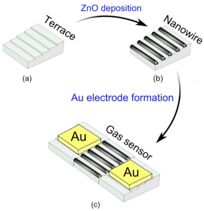
Diagram of the gas sensor fabrication process: (a) Uniform terraces formed on the (0001) sapphire substrate, (b) nanowires growth on the terrace using the laser pulsed layer deposition method, (c) nanowire-based gas sensor on the terrace. Reproduced with permission from Kim and Son [316]. Copyright 2009: Institute of Physics.
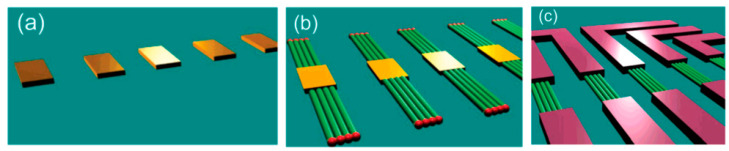
Schematic of the photolithography process for a scalable fabrication of nanowire devices. (a) Gold pads and fiducial marks are deposited on the surface. (b) NWs are grown selectively from the two sides of the gold pads. (c) Metal electrodes and bonding pads are placed exactly on NWs by the alignment of fiducial marks. Reproduced with permission from Nikoobakht [319]. Copyright 2007: American Chemical Society.
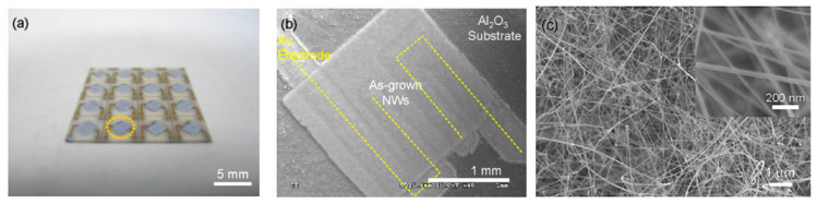
The sensor elements: (a) 16 sensor elements prepared by the one-pot growth of SnO2 nanowire networks on laser-scriber Al2O3 substrates; (b) SEM image of one sensor element; (c) SEM image of SnO2 nanowire networks. Reproduced with permission from Hwang et al. [153]. Copyright 2012: Elsevier.
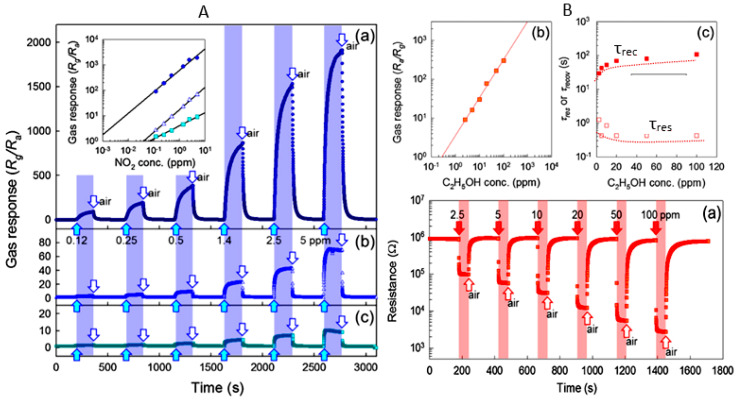
(A) Dynamic sensing transients to 0.12–5 ppm NO2 at (a) 141, (b) 190, and (c) 240 °C and the corresponding sensor response as a function of NO2 concentration (insert); (B) (a) dynamic sensing transients to 2.5–100 ppm C2H5OH, (b) gas responses as a function of the C2H5OH concentration, and (c) the 90% response times (τres) and 90% recovery times (τrec). Reproduced with permission from Hwang et al. [153]. Copyright 2012: Elsevier.
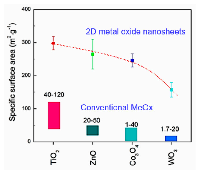
Typical specific surface areas of conventional metal oxide nanoparticles and 2D metal oxide nanosheets. Reproduced from Sun et al. [335]. Published by Nature Research as open access.
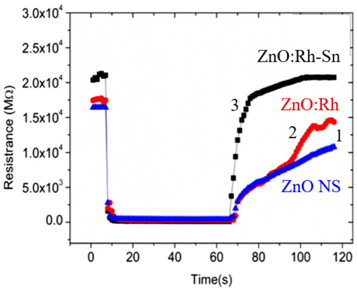
The response and recovery curves of different sensors to 100 ppm ethanol at an optimum working temperature (300 °C): 1—ZnO nanosheets; 2—ZnO:Rh; 3—ZnO:Rh-Sn. Reproduced from Sun et al. [335]. Published by Nature Research as open access.
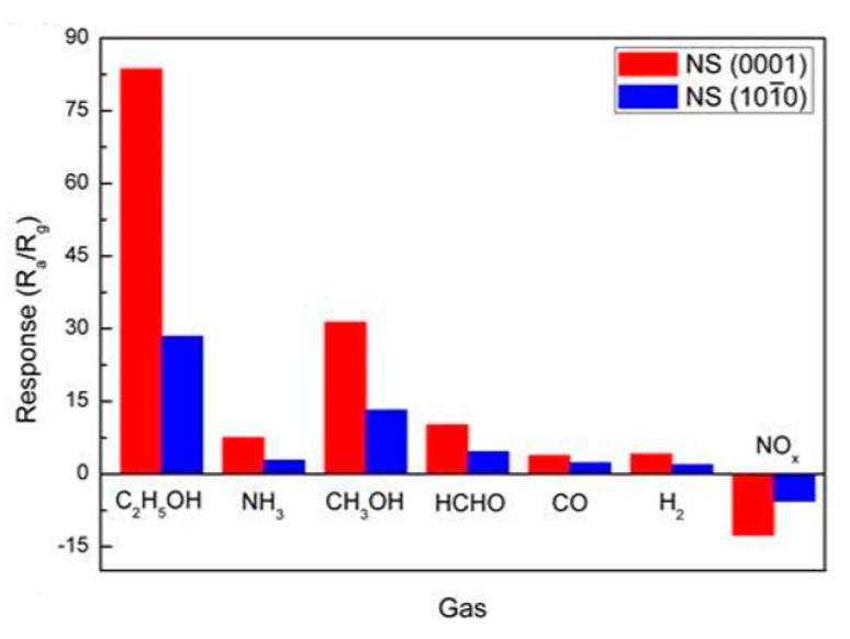
Response of ZnO nanosheets-based sensors to different gases. ZnO nanosheets in these sensors are faceted by different crystallographic planes, (0001) and ± (010), respectively. Reproduced with permission from Xu et al. [200]. Copyright 2017: Elsevier.
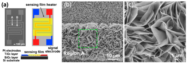
(a) Schematic diagrams of the different views for the microstructure sensor. Morphologies and crystal structures of ZnO nanosheets (NSs): (b,c) FESEM images of ZnO NSs taken from different regions in the microstructure sensor. Reproduced with permission from Zeng et al. [363]. Copyright 2012: Elsevier.

Low and high magnification (inset) FESEM images of WO3 (a) and Co3O4 nanosheets (b). Nanosheets were synthesized via a hydrothermal method. The thickness of nanosheets was from 20 to 30 nm for WO3 and from 20 to 50 nm for Co3O4 nanosheets. (a) Reproduced with permission from Wang et al. [368]. Copyright 2017: Elsevier; (b) reproduced with permission from Wang et al. [387]. Copyright 2015: Royal Society of Chemistry.
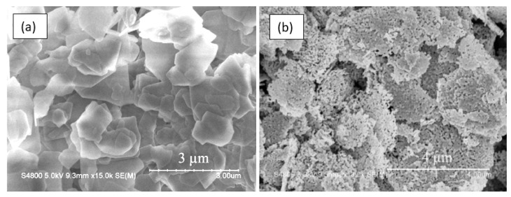
SEM images of (a) the as-synthesized BZN nanosheets, and (b) porous ZnO nanosheets after BZN nanosheets annealing at 300 °C. The thickness of nanosheets before annealing was in the range of 12–20 nm, and < 15 nm after annealing. Reproduced with permission from Huang et al. [401]. Copyright 2011: Elsevier.
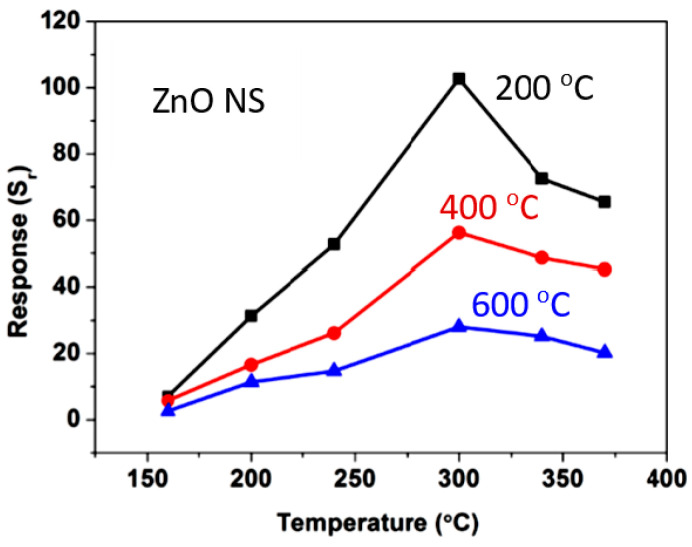
The operating temperature influence on the conductivity response to acetone vapor (200 ppm) of gas sensors based on ZnO nanosheets calcinated at 200, 400, and 600 °C. Reproduced with permission from Li et al. [374]. Copyright 2017: Elsevier.
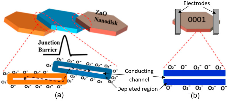
Schematic representation of the sensing mechanism in ZnO gas sensors fabricated using (a) a stack of ZnO nanodisks and (b) an individual nanodisk. Reproduced with permission from Alenezi et al. [402]. Copyright 2014: American Chemical Society.
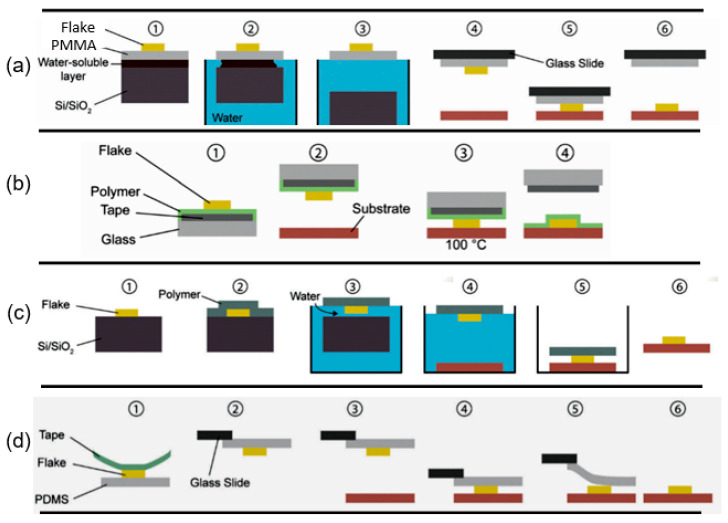
Illustration of transfer methods: (a) The PMMA carrying layer transfer method. The designated flake to be transferred is exfoliated onto a Si/SiO2 substrate which has been coated with a water-soluble polymer layer and PMMA (1). The stack is then immersed in water (2) where the water-soluble layer can dissolve leaving the PMMA layer carrying the flake floating on the water surface (3). The PMMA is then attached to a glass slide connected to a micromanipulator with the flake facing down (4). With the help of a microscope the flake is aligned with the target substrate and is then brought in contact (5). By gently separating the PMMA from the final substrate the flake gets transferred. (b) The Elvacite sacrificial layer transfer method. The target flake is exfoliated onto a layer of Evalcite deposited onto an adhesive tape attached to a glass slide (1). The stack is then positioned onto a target substrate and the flake is aligned with pre-existing features of the substrate (2). The substrate is heated up at 100 °C and the stack can then be brought in contact with the hot substrate (3) which melts the Evalcite layer leaving the capped flake on the final substrate (4). (c) The wedging transfer method. The flake to be transferred is exfoliated onto a hydrophilic substrate such as Si/SiO2 (1) and then covered by a layer of hydrophobic polymer (2). The stack is then immersed in water where the water molecules can intercalate between the SiO2 and the polymer carrying the flake (3). The polymer film carrying the flake remains floating on the water surface where it can be aligned with the help of a needle to the final substrate (4). By pumping down the water the two can be brought in contact (5). Then, the polymer can be dissolved leaving the flake transferred onto the final substrate (6). (d) The PDMS dry transfer method. The flake to be transferred is exfoliated onto a PDMS stamp (1) and the stamp is then attached to a glass slide connected to a micromanipulator (2). Using a microscope, the flake can be aligned with the final substrate (3) and brought in contact (4). By slowly peeling the PDMS stamp (5) the flake can be deposited on the substrate (6). Reproduced with permission from Frisenda et al. [403]. Copyright 2018: Royal Society of Chemistry.
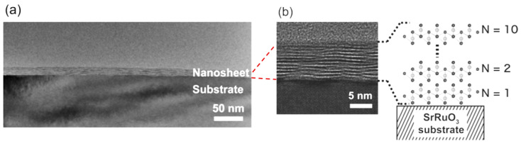
Cross-sectional TEM images of the 10-layer film of Ti0.87O2 nanosheets formed using the LB deposition technique: (a) Wide view; (b) magnified image. Reproduced with permission from Akatsuka et al. [405]. Copyright 2009: American Chemical Society.
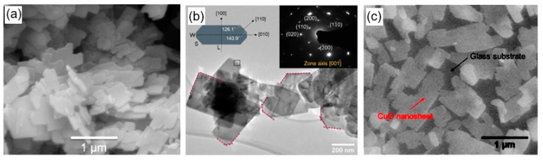
(a) SEM images of as-synthesized CuO nanosheets; (b) low-magnification TEM image of CuO nanosheets and the SAED pattern and a sketch of the crystal orientation in the real space as inset; (c) top surface SEM image of the CuO nanosheet monolayer on the glass substrate. Reproduced from Miao et al. [406]. Published by ACS as open access.
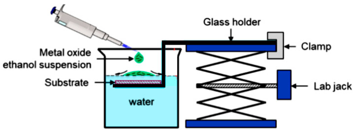
Illustration of the monolayer film formation process using the home-built coater. The red box illustrates that the CuO nanosheets float on the water surface due to the formation of a negative meniscus at the edges and self-assembly due to the attraction force of the same type of meniscus. Reproduced from Miao et al. [406]. Published by ACS as open access.
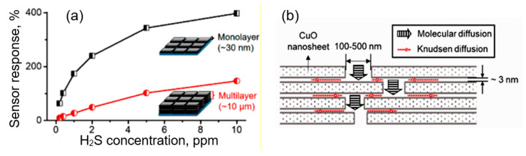
(a) Sensor response of monolayer- and multilayer-based sensors to H2S; (b) model of a multilayer film with lamellar structure. Reproduced from Miao et al. [406]. Published by ACS as open access.
References
-
- Lu J.G., Chang P.C., Fan Z.Y. Quasi-one-dimensional metal oxide materials—Synthesis, properties and applications. Mater. Sci. Eng. R. 2006;52:49–91. doi: 10.1016/j.mser.2006.04.002. - DOI
-
- Comini E., Baratto C., Faglia G., Ferroni M., Vomiero A., Sberveglieri G. Quasi-one dimensional metal oxide semiconductors: Preparation, characterization and application as chemical sensors. Prog. Mater. Sci. 2009;54:1–67. doi: 10.1016/j.pmatsci.2008.06.003. - DOI
Publication types
Grants and funding
LinkOut - more resources
Full Text Sources
Other Literature Sources
