

Nanocube Imprint Lithography
- PMID: 32806024
- PMCID: PMC7513471
- DOI: 10.1021/acsnano.0c04793
Nanocube Imprint Lithography
Abstract
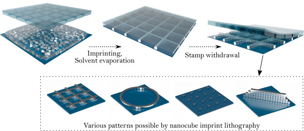
In recent years, imprint lithography has emerged as a promising patterning technique capable of high-speed and volume production. In this work, we report highly reproducible one-step printing of metal nanocubes. A dried film of monocrystalline silver cubes serves as the resist, and a soft polydimethylsiloxane stamp directly imprints the final pattern. The use of atomically smooth and sharp faceted nanocubes facilitates the printing of high-resolution and well-defined patterns with face-to-face alignment between adjacent cubes. It also permits digital control over the line width of patterns such as straight lines, curves, and complex junctions over an area of several square millimeters. Single-particle lattices as well as three-dimensional nanopatterns are also demonstrated with an aspect ratio up to 5 in the vertical direction. The high-fidelity nanocube patterning combined with the previously demonstrated epitaxial overgrowth can enable curved (single) crystals from solution at room temperature or highly efficient transparent conductors.
Keywords: PDMS; assembly; colloidal ink; large-scale printing; nanocubes; patterning.
Conflict of interest statement
The authors declare no competing financial interest.
Figures


References
-
- Pimpin A.; Srituravanich W. Review on Micro- and Nanolithography Techniques and Their Applications. Eng. J. 2012, 16, 37–56. 10.4186/ej.2012.16.1.37. - DOI
-
- Kumar A.; Whitesides G. M. Features of Gold Having Micrometer to Centimeter Dimensions Can Be Formed through a Combination of Stamping with an Elastomeric Stamp and an Alkanethiol ‘“Ink”’ Followed by Chemical Etching. Appl. Phys. Lett. 1993, 63, 2002–2004. 10.1063/1.110628. - DOI
-
- Wilbur J. L.; Kumar A.; Kim E.; Whitesides G. M. Microfabrication by Microcontact Printing of Self-Assembled Monolayers. Adv. Mater. 1994, 6, 600–604. 10.1002/adma.19940060719. - DOI
LinkOut - more resources
Full Text Sources
