Review
. 2020 Aug 25;25(17):3856.
doi: 10.3390/molecules25173856.

Chemical Vapour Deposition of Graphene-Synthesis, Characterisation, and Applications: A Review

Affiliations
Review

Chemical Vapour Deposition of Graphene-Synthesis, Characterisation, and Applications: A Review

Maryam Saeed et al. Molecules. .

Abstract

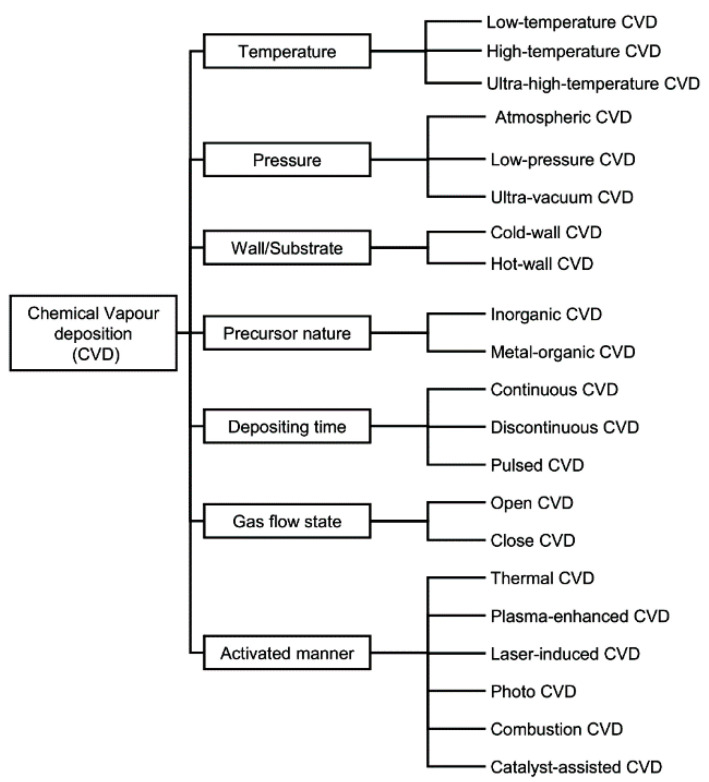
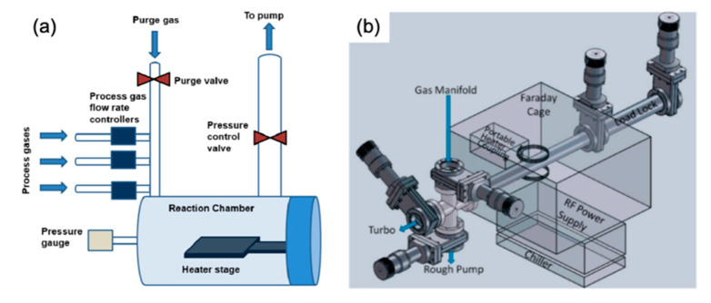
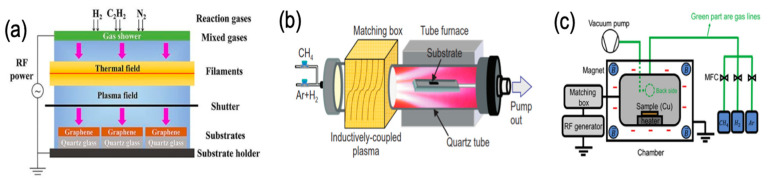
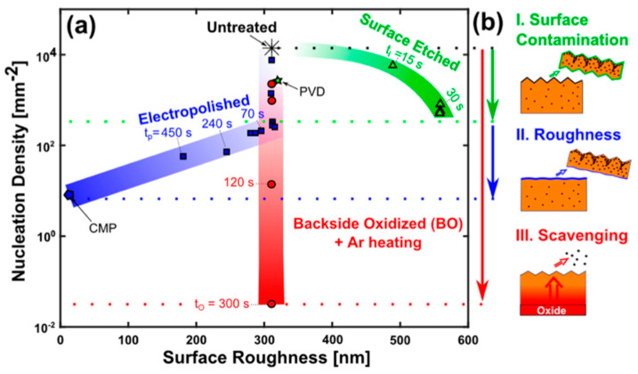
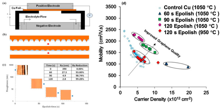
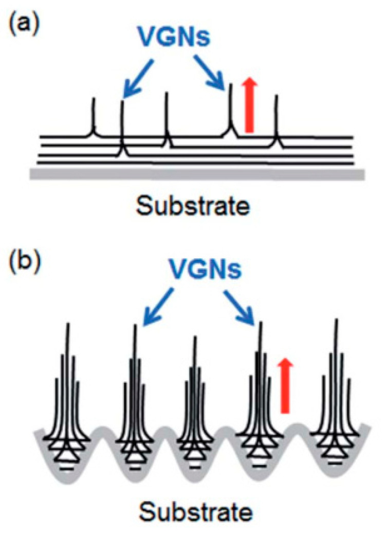
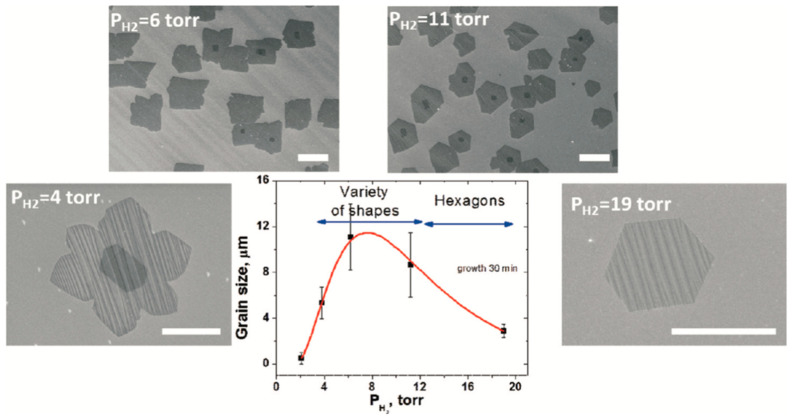
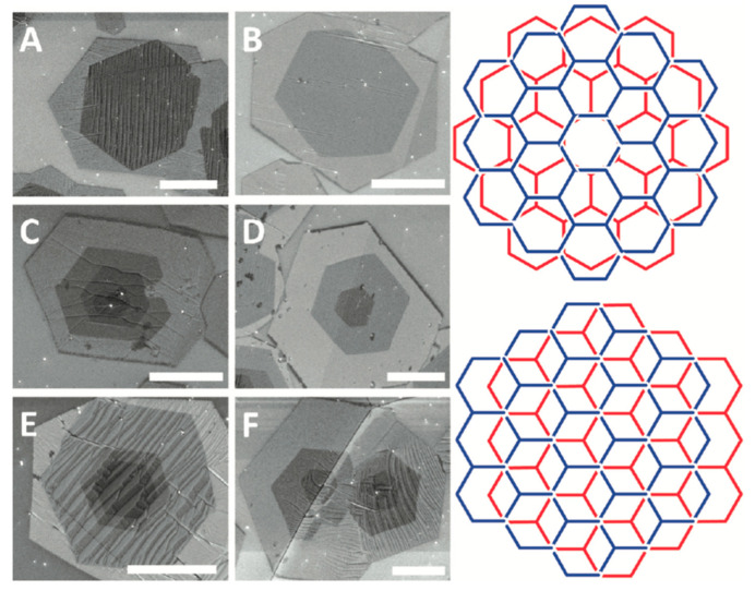
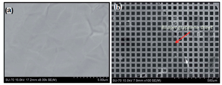
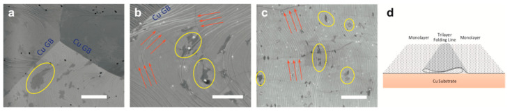
Graphene as the 2D material with extraordinary properties has attracted the interest of research communities to master the synthesis of this remarkable material at a large scale without sacrificing the quality. Although Top-Down and Bottom-Up approaches produce graphene of different quality, chemical vapour deposition (CVD) stands as the most promising technique. This review details the leading CVD methods for graphene growth, including hot-wall, cold-wall and plasma-enhanced CVD. The role of process conditions and growth substrates on the nucleation and growth of graphene film are thoroughly discussed. The essential characterisation techniques in the study of CVD-grown graphene are reported, highlighting the characteristics of a sample which can be extracted from those techniques. This review also offers a brief overview of the applications to which CVD-grown graphene is well-suited, drawing particular attention to its potential in the sectors of energy and electronic devices.

Keywords: CVD; NEMS; characterisation; deposition; flexible electronics; graphene; growth.


Conflict of interest statement

The authors declare no conflict of interest.

Figures

Figure 1
Figure 1
Classification of CVD methods (reprinted with permission from [23]).
Figure 2
Figure 2
Schematic diagram of a typical hot-wall horizontal tube-furnace CVD system (LP: low pressure, AP: atmospheric pressure).
Figure 3
Figure 3
Schematic diagram of thermal CVD growth of graphene.
Figure 4
Figure 4
SEM images illustrate the evolution of the shape of graphene domains using different H2/CH4 ratios. (ah), H2/CH4 ratios are 20, 30, 40, 60, 70, 80, 100 and 120, respectively, while the CH4 flow rate is kept constant at 0.5 sccm. The flow rates of H2/CH4 for (il) are 200/2, 200/4, 300/5 and 300/22 sccm, respectively. All scale bars are 5 µm (reprinted with permission from [63]).
Figure 5
Figure 5
Coverage type for CVD of graphene versus growth temperature and pressure of active species as reported in the literature and Lewis et al. study. The data points span a range of different RCH denoted by the color: black: 1 > RCH > 0.1; gray for 0.1 > RCH > 0.01; purple for 0.01 > RCH > 0.001 and blue for 0.001 > RCH > 0.0001. The red data points correspond to the work done by Lewis et al., where RCH = 0.2 (reprinted with permission from [65]).
Figure 6
Figure 6
Flow rate of acetylene as the hydrocarbon feedstock versus the diameter and the number of layers produced in CVD has grown graphene (reprinted with permission from [66]).
Figure 7
Figure 7
Analysis plots showing (a) nucleation density versus growth temperature, (b) nucleus growth rate versus growth temperature (reprinted with permission from [78]).
Figure 8
Figure 8
Raman spectra of the CVD grown graphene samples as a function of temperature (reprinted with permission from [79]).
Figure 9
Figure 9
(a) a scheme of the cold wall CVD system used for graphene growth [81] and (b) the cold wall CVD system based on radio frequency magnetic inductive heating (reprinted with permission from [85]).
Figure 10
Figure 10
Diagram of the resistively heated stage cold wall CVD system (reprinted with permission from [88]).
Figure 11
Figure 11
A schematic of a general PECVD setup (reprinted with permission from [95]).
Figure 12
Figure 12
A schematic of (a) MW-PECVD setup and (b) the zoom-in of the growth of graphene (reprinted with permission from [96]).
Figure 13
Figure 13
A schematic of the RF-PECVD setup accompanied with (a) hot filament [106], (b) ICP [107] and (c) CCP (reprinted with permission from [112]).
Figure 14
Figure 14
(a) overview of Cu pre-treatments and the effect on graphene nucleation density and Cu surface roughness; (b) schematic indicating the cause of the reduction in nucleation density for surface pre-treatments I−III (reprinted with permission from [125]).
Figure 15
Figure 15
Schematic of (a) EP setup and (b) planarization mechanism during polishing. (c) AFM images showing as received Cu compared to EP Cu using different EP times. The inset table displays the measured surface roughness of the EP samples over time and the reduction rate from the as-received sample (reprinted with permission from [130]); (d) a plot of mobility versus carrier density of CVD grown graphene on EP Cu (reprinted with permission from [131]).
Figure 16
Figure 16
Scheme for the mechanism of VGN growth on (a) untreated and (b) Ar plasma-treated substrates (reprinted with permission from [132]).
Figure 17
Figure 17
OES of the Cu reduction after 1 and 10 min of the exposure to hydrogen plasma, showing the reduction of the OH peaks that indicates the reduction and removal of the native oxide layer on the surface of Cu substrate (reprinted with permission from [77]).
Figure 18
Figure 18
(a) FESEM image recorded at the interface of Ni (left) and graphene/Ni (right). The absence and presence of graphene in two regions are confirmed with the EDAX spectra shown below them. The circles represent the scenarios in (b) and (d) where grain boundaries meet. A FESEM and AFM image of annealed Ni foil (b,c) and graphene peeled-off Ni foil (d,e). z-scale: 1 μm. Dashed lines are drawn for easy guide. (reprinted with permission from [136]).
Figure 19
Figure 19
Difference in graphene growth processes between (a) Cu and (b) Ni substrates. Surface diffusion occurs on Cu substrate while bulk diffusion and precipitation occurs on Ni (reprinted with permission from [115]).
Figure 20
Figure 20
Schematic illustration of the carbon distribution in (a) liquid Cu, (b) solidified surface of the liquid Cu and (c) solid Cu. (d) XPS composition profile showing elements (O, C and Cu) along the surface after CVD graphene growth showing a larger amount of C dissolved in bulk, demonstrating the increase in carbon solubility in Cu at its liquid state (reprinted with permission from [149]).
Figure 21
Figure 21
(a) characteristic Raman spectra of graphene and (b) Raman scattering processes (reprinted with permission from [186]).
Figure 22
Figure 22
(a) comparison of the Raman spectra of graphene and graphite using a 514 nm excitation wavelength. (b) a close-up comparison of the 2D peaks in graphene and graphite (reprinted with permission from [184]); (c) measured 2D Raman band of different graphene layers showing the splitting of the 2D band which opens up as it goes from 1-LG to 3-LG and then closes up as it goes from 4-LG to highly oriented pyrolytic graphite (HOPG), (514 nm excitation wavelength) (reprinted with permission from [186]).
Figure 23
Figure 23
(a,b) comparison of the Raman spectra of G (2D) and G* bands of monolayer graphene showing linearly blue shifts of the G’ band with increasing excitation energy (the circles correspond to graphene, and the diamonds correspond to turbostratic graphite); (c,d) the change of the 2D peak shape as a function of the number of graphene layers are shown for 514 and 633 nm excitations, respectively (reprinted with permission from [184,186]).
Figure 24
Figure 24
(a) illustration of Raman spectra of graphene oxide (GO) as a function of the distance between defects (reprinted with permission from [192]); (b) the ratio of ID/IG from different monolayer graphene samples as a function of the average distance LD between defects that are induced by the Ar+ ion bombardment, the inset ratio of ID/IG versus LD for two graphite samples (reprinted with permission from [193]).
Figure 25
Figure 25
SEM images showing the morphology of the obtained graphene domains as a function of hydrogen partial pressure and its effect on grain size. Scale bars are 10 µm (top two images) and 2 µm (bottom two images) (reprinted with permission from [61]).
Figure 26
Figure 26
Analysis of mutual orientation between the layers in multi-layered graphene grown for 30 min at 60 ppm CH4, 19 Torr hydrogen pressure. All layers have hexagonal shapes in distinct contrast to irregular grains at higher methane concentrations. The second layer often appears misoriented with respect to the first layer, frequently showing 30 degrees rotation (right graphic) (A,B,E), while some do show what resembles AB Bernal stacking (C,D). The third and fourth layers, on the other hand, always show AB stacking (C,F). Scale bars are 3 µm (reprinted with permission from [61]).
Figure 27
Figure 27
(a) FESEM image of the as-grown graphene films on Cu; (b) high-magnification FESEM image of a bilayer graphene sheet on a Cu grid, prepared by hot filament thermal CVD (reprinted with permission from [193]).
Figure 28
Figure 28
SEM images of CVD has grown graphene on Cu using different detectors (a) backscattering, (b) ETD and (c) TLD. Yellow circles present few-layer graphene, red arrows show the graphene folding lines and the blue Cu GB text present a Cu grain boundary. Scale bars for a–c are 5 µm; (d) a schematic illustration of a folding line (reprinted with permission from [138]).
Figure 29
Figure 29
SEM images of VAGNAs at different CH4 ratios using PECVD, showing the variation in thickness (reprinted with permission from [101]).
Figure 30
Figure 30
(a) SEM image showing the ripples in the graphene surface (4 ripples/1 µm); (b) AFM image of the formation of ripples in graphene; (c) height profile of the two sections shown in (b); (d) section showing a profile of an ideal thermal groove (reprinted with permission from [78]).
Figure 31
Figure 31
AFM images showing surface topography with a quantitative height line scan across hexagonal growth defects on graphene films grown on Cu/Mo substrate using APCVD (reprinted with permission from [49]).
Figure 32
Figure 32
AFM images of (a) super-clean graphene freshly grown on Cu substrate, and transferred graphene on target substrate (b) unclean graphene and (c) super clean graphene (reprinted with permission from [203]).
Figure 33
Figure 33
TEM images of CVD grown graphene showing different thicknesses, (a) 1 layer, (b) 3 layers, (c) 4 layers and (d) 8 layers. (reprinted with permission from [43]).
Figure 34
Figure 34
TEM analysis of CVD graphene flake from ethanol prepared with 4 h growth time. The HRTEM image showing both monolayer and bilayer graphene regions Moire patterns as a result of rotational misalignment of the two graphene layers are observed in the bilayer region. Hexagonal selected area electron diffraction patterns of the monolayer and bilayer graphene reveal the superior crystallinity. Their representative Raman spectra are illustrated in the bottom panel with I2D/IG ratio of 1.88 and 1.26 for 1 L and 2 L, respectively (reprinted with permission from [209]).
Figure 35
Figure 35
Computer simulation of HRTEM contrast showing zigzag and armchair ribbons of monolayer graphene layers (reprinted with permission from [210]).
Figure 36
Figure 36
(a,b) illustrate the TEM a defect formed by rotating a carbon-carbon bond by 90° and its atomic structure as obtained from DFT calculations, respectively [211]. (c,d) show a single vacancy by experimental TEM and its atomic structure obtained by DFT calculation, respectively. (e) aberration-corrected annular dark-field STEM of line defects in graphene [216]; (fi) jumping of foreign W atom (arrowed) on the surface of few-layer graphene eat 480 °C using in situ HRTEM, the repeating jumping between the trapping sites (1 and 2) at a distance of 1.5 nm shows the attraction between the metal adatom and the defect (reprinted with permission from [211]).

References

    1. Novoselov K.S., Geim A.K., Morozov S.V., Jiang D., Zhang Y., Dubonos S.V., Grigorieva I.V., Firsov A.A. Electric field effect in atomically thin carbon films. Science. 2004;306:666–669. doi: 10.1126/science.1102896. - DOI - PubMed
    1. Novoselov K.S., Geim A.K. The rise of graphene.pdf. Nat. Mater. 2007;6:183–191. - PubMed
    1. Bonaccorso F., Colombo L., Yu G., Stoller M., Tozzini V., Ferrari A.C., Ruoff R.S., Pellegrini V. Graphene, related two-dimensional crystals, and hybrid systems for energy conversion and storage. Science. 2015;347:1246501. doi: 10.1126/science.1246501. - DOI - PubMed
    1. Morozov S.V., Novoselov K.S., Katsnelson M.I., Schedin F., Elias D.C., Jaszczak J.A., Geim A.K. Giant intrinsic carrier mobilities in graphene and its bilayer. Phys. Rev. Lett. 2008;100:016602. doi: 10.1103/PhysRevLett.100.016602. - DOI - PubMed
    1. Wang N., Samani M.K., Li H., Dong L., Zhang Z., Su P., Chen S., Chen J., Huang S., Yuan G., et al. Tailoring the thermal and mechanical properties of graphene film by structural engineering. Small. 2018;14:1801346. doi: 10.1002/smll.201801346. - DOI - PubMed

LinkOut - more resources