Review
. 2020 Aug 26;13(17):3774.
doi: 10.3390/ma13173774.

Writing 3D Nanomagnets Using Focused Electron Beams

Affiliations
Review

Writing 3D Nanomagnets Using Focused Electron Beams

Amalio Fernández-Pacheco et al. Materials (Basel). .

Abstract

Focused electron beam induced deposition (FEBID) is a direct-write nanofabrication technique able to pattern three-dimensional magnetic nanostructures at resolutions comparable to the characteristic magnetic length scales. FEBID is thus a powerful tool for 3D nanomagnetism which enables unique fundamental studies involving complex 3D geometries, as well as nano-prototyping and specialized applications compatible with low throughputs. In this focused review, we discuss recent developments of this technique for applications in 3D nanomagnetism, namely the substantial progress on FEBID computational methods, and new routes followed to tune the magnetic properties of ferromagnetic FEBID materials. We also review a selection of recent works involving FEBID 3D nanostructures in areas such as scanning probe microscopy sensing, magnetic frustration phenomena, curvilinear magnetism, magnonics and fluxonics, offering a wide perspective of the important role FEBID is likely to have in the coming years in the study of new phenomena involving 3D magnetic nanostructures.

Keywords: 3D printing; additive manufacturing; focused electron beam; lithography; magnetic nanowires; nanofabrication; nanomagnetism; spintronics.


Conflict of interest statement

The authors declare no conflict of interest.

Figures
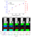
Figure 4
Figure 4
Scanning transmission electron microscopy characterization of Co nanowires under an annealing post-growth purification process. (a) Average B-field and Co composition as a function of annealing temperature measured by off-axis electron holography. (b) High-angle annular dark-field and corresponding fast-Fourier-transform (first row), and chemical maps by electron energy loss spectroscopy (following rows). Scale bars are 20 nm. (c) Hysteresis loops obtained by nano-SQUID (super quantum interference device) magnetometry at 15 K for each of the wires. (a,b) Reproduced with permission from [52]. (c) Reproduced with permission from [55]. Copyright 2018 American Chemical Society.
Figure 1
Figure 1
(a) Schematics of focused electron beam induced deposition (FEBID) for 3D nano-patterning, where gas injected by a nozzle is adsorbed on a substrate, with a fraction getting decomposed by a focused beam of electrons. By controlling the time the beam dwells on each point, 3D nano-printing of magnetic materials becomes possible. Reproduced with permission from [16]. Copyright 2020 American Chemical Society. (b) Comparison of speed and resolution of FEBID and its sister technique focused ion beam induced deposition (FIBID), with other emerging additive manufacturing methods for the direct writing of metallic micro- and nano- structures. FEBID at cryogenic temperatures (cryo-FEBID) enables direct-writing at very high growth rates, with slightly worse resolution [17,18]; a similar resolution as cryo-FEBID, with an approximately 100 increase in growth rate has been recently demonstrated using cryo-FIBID [19,20] (not shown here). Adapted with permission from [21].
Figure 2
Figure 2
(a) Exemplary 3D computer-aided design (CAD) model of a ferromagnetic tetrapod structure with slicer plane for 2D pattern generation, for illustration. (b) Result of Monte Carlo simulation of several primary electron trajectories at 20 keV energy for tetrapod structure illustrating elastic scattering (yellow trajectories) and deposited energy (colour bar), due to inelastic scattering. (c) Temperature distribution in tetrapod structure under electron beam exposure at 20 keV and 44 pA beam current, when the electron beam hits at the topmost upper front arm (stationary state finite difference solution of heat conduction equation). The temperature increase is from 293 K at the base of the structure to about 303 K at the beam impact position; material parameters of Pt20C80.
Figure 3
Figure 3
(a) An array of vertical pillars is built with varying deposition times. The height of the resulting structures is used to determine the base growth rate, and temperature scaling factor, reducing the growth rate as pillars get longer. (b) The effective standard deviation σ of the deposit is determined by comparing wide nanowires to a single pixel line (SPL), allowing correction for proximity effects. (c) Stereolithography (STL) model of a human hand. (d,e) Side and top view SEM images of the model fabricated with MeCpPt(Me)3. (f,g) Ferromagnetic Möbius strip made using Co2(CO)8, where arrows are included to help visualize the geometry. Scale bars are 1 µm. Adapted with permission from [16]. Copyright 2020 American Chemical Society.
Figure 5
Figure 5
Fabrication and characterization of 3D FEBID-PVD (physical vapor deposition) hybrid nanostructures. (a) Non-magnetic FEBID scaffold fabricated with the MeCpPt(Me)3 precursor. (b) Permalloy evaporation onto the structure. (c) Schematic of the resulting nanomagnetic system. The 2D film acts as the source of domain walls which can be injected into the nanowire via the 2D-3D interconnect. (d) SEM image of the fabricated nanowire. Scale bar is 1 µm. (e) External magnetic fields applied as a function of time. The coordinate system is defined with x being along the length of the nanowire and y being parallel to the film (see c). A transverse field (Hy) (is employed as a magnetic gate to control the injection of domain from the film transmitted by the rotating Hx and Hz fields. (f) Magnetic switching of the nanowire via domain wall motion, probed by dark-field magneto-optical Kerr effect. Adapted with permission from [65]. Copyright 2017 American Chemical Society.
Figure 6
Figure 6
SEM micrographs of the three types of magnetic sensors grown by FEBID on cantilevers for scanning probe microscopy. (a) Co nanosphere on a cantilever for ferromagnetic resonance force microscopy. (b) Fe tip for magnetic force microscopy. (c) Long Co nanowire for scanning magnetic force sensing. (a) Reproduced with permission from [71]. (c) Reprinted with permission from [73]. Copyright 2020 by the American Physical Society.
Figure 7
Figure 7
(a) Schematic of typical gradiometry setup for micro-Hall magnetometry with a tetrapod 3D ferromagnetic structure fabricated by FEBID; see [85] for details. From the measured Hall voltages VH(s) and VH(r), the magnetic stray field generated by the tetrapod can be deduced. (b) Energy diagram of a tetrapod structure assuming uniformly magnetized arms within the dumbbell approximation. The sixfold degenerate ground state refers to the “two in – two out” ice rule for tetrahedral spin ice [86]. Configuration #4 shown in the inset depicts one of the possible ground states. (c) Macrospin model for the tetrapod with uniaxial anisotropy along the arm directions in zero field, where a “two in–two out” state is realized. (d) Result of zero-field micromagnetic simulation of tetrapod structure using mumax3 [85] with material parameters of Co3Fe; see [85] for details. The colour code on the plane of the 2DEG represents the z-component of the magnetic stray field generated by the tetrapod. (e) Comparison of results of stray field calculations for Co3Fe tetrapod with field perpendicular to the 2DEG. Micromagnetic (red) and macro-spin (blue) simulation show roughly corresponding coercive fields but clear differences in details of the stray field hysteresis. Suitable parameter selection for the macro-spin simulation can reduce these differences to some degree; see [28] for details.
Figure 8
Figure 8
(a) Double-helix with opposite chirality (bottom LH: left-handed; top RH: right-handed) interfaced at the region marked by an asterisk. Scale bar is 1 µm. (b,c) Micromagnetic simulations of the double-helix system in an antiparallel magnetic state; a Bloch wall with a well-defined chirality is formed between the strands, with the chirality defined by the chirality of the corresponding helix. A 3D vortex with a Néel defect is formed at the region (*) connecting both chiralities. Reproduced with permission from [98]. Copyright 2020 American Chemical Society.
Figure 9
Figure 9
Atomic force microscopy images of exemplary FEBID structures for fluxonics and magnonics. (a) Nb film decorated with an array of asymmetrically shaped Co nanostripes inducing a ratchet pinning potential landscape of the washboard type for Abrikosov vortices. (b) Bi-periodic magnonic crystal on the surface of a Py film that allows for reprogramming the band structure in the magnon frequency spectrum. (c) Magnonic waveguide with a gradually decreasing thickness that induces a graded refractive index for spin waves via the magnetization gradient. (d) 3D magnonic crystal in which the thickness modulation period is a factor of two larger than the width modulation period. (e) Y-shaped magnonic waveguide with a nanogroove milled by focused ion beam (FIB) at the junction for frequency-selective steering of spin waves via the refraction and reflection effects. (f) “Nano-volcano” for ferromagnetic resonance studies. Structures (bf) are fabricated from Co3Fe employing the precursor HFeCo3(CO)12.

References

    1. Baibich M.N., Broto J.M., Fert A., Van Dau F.N., Petroff F., Eitenne P., Creuzet G., Friederich A., Chazelas J. Giant magnetoresistance of (001)Fe/(001)Cr magnetic superlattices. Phys. Rev. Lett. 1988;61:2472–2475. doi: 10.1103/PhysRevLett.61.2472. - DOI - PubMed
    1. Fert A., Campbell I.A. Transport Properties of Ferromagnetic Transition Metals. J. Phys. Colloq. 1971;32:C1-46–C1-50. doi: 10.1051/jphyscol:1971109. - DOI
    1. Beach G.S.D., Tsoi M., Erskine J.L. Current-induced domain wall motion. J. Magn. Magn. Mater. 2008;320:1272–1281. doi: 10.1016/j.jmmm.2007.12.021. - DOI
    1. Emori S., Bauer U., Ahn S.-M., Martinez E., Beach G.S.D. Current-driven dynamics of chiral ferromagnetic domain walls. Nat. Mater. 2013;12:611–616. doi: 10.1038/nmat3675. - DOI - PubMed
    1. Fernández-Pacheco A., Streubel R., Fruchart O., Hertel R., Fischer P., Cowburn R.P. Three-dimensional nanomagnetism. Nat. Commun. 2017;8:15756. doi: 10.1038/ncomms15756. - DOI - PMC - PubMed

LinkOut - more resources