Camphor-Based CVD Bilayer Graphene/Si Heterostructures for Self-Powered and Broadband Photodetection
- PMID: 32867054
- PMCID: PMC7570377
- DOI: 10.3390/mi11090812
Camphor-Based CVD Bilayer Graphene/Si Heterostructures for Self-Powered and Broadband Photodetection
Abstract
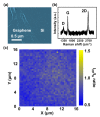
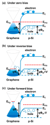
This work demonstrates a self-powered and broadband photodetector using a heterojunction formed by camphor-based chemical vaper deposition (CVD) bilayer graphene on p-Si substrates. Here, graphene/p-Si heterostructures and graphene layers serve as ultra-shallow junctions for UV absorption and zero bandgap junction materials (<Si bandgap (1.1 eV)) for long-wave near-infrared (LWNIR) absorption, respectively. According to the Raman spectra and large-area (16 × 16 μm2) Raman mapping, a low-defect, >95% coverage bilayer and high-uniformity graphene were successfully obtained by camphor-based CVD processes. Furthermore, the carrier mobility of the camphor-based CVD bilayer graphene at room temperature is 1.8 × 103 cm2/V·s. Due to the incorporation of camphor-based CVD graphene, the graphene/p-Si Schottky junctions show a good rectification property (rectification ratio of ~110 at ± 2 V) and good performance as a self-powered (under zero bias) photodetector from UV to LWNIR. The photocurrent to dark current ratio (PDCR) value is up to 230 at 0 V under white light illumination, and the detectivity (D*) is 8 × 10¹² cmHz1/2/W at 560 nm. Furthermore, the photodetector (PD) response/decay time (i.e., rise/fall time) is ~118/120 μs. These results support the camphor-based CVD bilayer graphene/Si Schottky PDs for use in self-powered and ultra-broadband light detection in the future.
Keywords: camphor-based CVD; graphene; graphene/Si PDs; self-power photodetector.
Conflict of interest statement
The authors declare no conflict of interest.
Figures


Similar articles
-
A Silicon Sub-Bandgap Near-Infrared Photodetector with High Detectivity Based on Textured Si/Au Nanoparticle Schottky Junctions Covered with Graphene Film.Sensors (Basel). 2023 Jul 6;23(13):6184. doi: 10.3390/s23136184. Sensors (Basel). 2023. PMID: 37448033 Free PMC article.
-
A low-cost broadband photodetector based on CsPbBr3quantum dots/transfer-free eco-friendly graphene heterostructures for fast photoresponse.Nanotechnology. 2025 May 28;36(23). doi: 10.1088/1361-6528/add899. Nanotechnology. 2025. PMID: 40367959
-
Self-Powered Broadband Photodetector Based on NiO/Si Heterojunction Incorporating Graphene Transparent Conducting Layer.Nanomaterials (Basel). 2024 Mar 21;14(6):551. doi: 10.3390/nano14060551. Nanomaterials (Basel). 2024. PMID: 38535699 Free PMC article.
-
Sensing of ultraviolet light: a transition from conventional to self-powered photodetector.Nanoscale. 2021 Oct 1;13(37):15526-15551. doi: 10.1039/d1nr04561j. Nanoscale. 2021. PMID: 34522938 Review.
-
Semimetals for high-performance photodetection.Nat Mater. 2020 Aug;19(8):830-837. doi: 10.1038/s41563-020-0715-7. Epub 2020 Jul 6. Nat Mater. 2020. PMID: 32632282 Review.
References
-
- Monroy E., Omnes F., Calle F. Wide-bandgap semiconductor ultraviolet photodetectors. Semicond. Sci. Technol. 2003;18:33–51. doi: 10.1088/0268-1242/18/4/201. - DOI
-
- Wei T.-C., Tsai D.-S., Ravagger P., Ke J.-J., Tsai M.-L., Lien D.-H., Huang C.-Y., Horng R.-H., He J.-H. See-through Ga2O3 solar-blind photodetectors for use in harsh environments. IEEE J. Sel. Top. Quant. Electron. 2014;20:112–117.
-
- Zhang Y., Ji T., Zhang W., Guan G., Ren Q., Xu K., Huang X., Zou R., Hu J. A self-powered broadband photodetector based on an n-Si (111)/p-NiO heterojunction with high photosensitivity and enhanced external quantum efficiency. J. Mater. Chem. C. 2017;5:12520–12528. doi: 10.1039/C7TC04565D. - DOI
-
- Thahe A.A., Bakhtiar H., Bidin N., Hassan Z., Qaeed M.A., Ramizy A., Talib Z.A., Ahmed N.M., Omar K., Alqaraghuli H., et al. High-performance nanoporous silicon-based photodetectors. Optik. 2018;168:424–431. doi: 10.1016/j.ijleo.2018.04.084. - DOI
LinkOut - more resources
Full Text Sources
Miscellaneous

