Review
. 2020 Aug 27;10(9):1689.
doi: 10.3390/nano10091689.

Surface and Interface Designs in Copper-Based Conductive Inks for Printed/Flexible Electronics

Affiliations
Review

Surface and Interface Designs in Copper-Based Conductive Inks for Printed/Flexible Electronics

Daisuke Tomotoshi et al. Nanomaterials (Basel). .

Abstract

Silver (Ag), gold (Au), and copper (Cu) have been utilized as metals for fabricating metal-based inks/pastes for printed/flexible electronics. Among them, Cu is the most promising candidate for metal-based inks/pastes. Cu has high intrinsic electrical/thermal conductivity, which is more cost-effective and abundant, as compared to Ag. Moreover, the migration tendency of Cu is less than that of Ag. Thus, recently, Cu-based inks/pastes have gained increasing attention as conductive inks/pastes for printed/flexible electronics. However, the disadvantages of Cu-based inks/pastes are their instability against oxidation under an ambient condition and tendency to form insulating layers of Cu oxide, such as cuprous oxide (Cu2O) and cupric oxide (CuO). The formation of the Cu oxidation causes a low conductivity in sintered Cu films and interferes with the sintering of Cu particles. In this review, we summarize the surface and interface designs for Cu-based conductive inks/pastes, in which the strategies for the oxidation resistance of Cu and low-temperature sintering are applied to produce highly conductive Cu patterns/electrodes on flexible substrates. First, we classify the Cu-based inks/pastes and briefly describe the surface oxidation behaviors of Cu. Next, we describe various surface control approaches for Cu-based inks/pastes to achieve both the oxidation resistance and low-temperature sintering to produce highly conductive Cu patterns/electrodes on flexible substrates. These surface control approaches include surface designs by polymers, small ligands, core-shell structures, and surface activation. Recently developed Cu-based mixed inks/pastes are also described, and the synergy effect in the mixed inks/pastes offers improved performances compared with the single use of each component. Finally, we offer our perspectives on Cu-based inks/pastes for future efforts.

Keywords: complexes; copper; flexible devices; inks; nanoparticles; pastes; printed electronics.


Conflict of interest statement

The authors declare no conflict of interest.

Figures

Figure 1
Figure 1
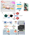
Strategies for Cu oxidation resistance and low-temperature sintering by the surface and interface designs in Cu-based conductive inks/pastes.
Figure 2
Figure 2
Categories of Cu-based inks/pastes.
Figure 3
Figure 3
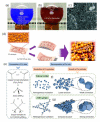
Mass fractions of Cu, Cu2O, and CuO in nanoparticles oxidized at (a) 170 °C and (b) 240 °C. Reprinted with permission from reference [31], Copyright Elsevier, 2011. Adsorption property calculation of (c) primary amine, (d) secondary amine, and (e) tertiary amine groups of polyethylenimine (PEI) with a Cu (111) surface. Reprinted with permission from reference [38], Copyright American Chemical Society, 2018. (f) Schematic representation of the ligand exchange process where oleylamine (OAM) attached to the CuNPs is replaced by incoming thiol ligand. (g) Molecular structures of OAM and the thiols used for ligand exchange and capping of Cu nanoparticles sorted according to the chain length and stability in the air. Reprinted with permission from reference [39], Copyright Springer Nature, 2017.
Figure 4
Figure 4
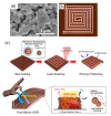
(a) Schematics of the photonic drying and sintering process of Cu nano ink, using near-infrared (NIR), flash white light, and deep UV. (b) The morphological change of Cu nanoparticles in nano ink during the photonic drying and sintering process. Reprinted with permission from reference [51], Copyright Springer Nature, 2016. (c) Schematic fabrication process: a randomly patterned master mold is used for pattern transfer onto the polyethylene terephthalate (PET) film using UV-curable epoxy. Cu nanoparticles (Cu NPs) are filled in the trench. The nanoparticles are treated with lactic acid and sintered by the thermal conduction layer (TCL)-assisted laser sintering process. The microscopic image of the (d) conventional laser-sintered electrode and (e) TCL-assisted laser-sintered electrode (TCITE). The inset images depict relative heat transfer rates between materials. (f) Highly transparent fabricated electrode. (g) Narrow line width (~2.4 μm) of the fabricated electrode. (h) TCITE overlaid on high-resolution (518 ppi) display. Reprinted with permission from reference [55], Copyright American Chemical Society, 2019. Schematic diagram of the plasma process (i) and Cu pattern photos before and after plasma treatment (j). Reprinted with permission from reference [56], Copyright Royal Society of Chemistry, 2015.
Figure 5
Figure 5
(a) Schematic of the necking and connection formation between the Cu fine particles using our two-step annealing process. SEM images of the Cu particle layer surface after oxidative annealing. (b) An SE (secondary electron) image and (c) a BEI-COMPO image with the red arrows marking the areas of organic material. Reprinted with permission from reference [58], Copyright Royal Society of Chemistry, 2015. (d) Electrical resistivity of Cu conductive patterns annealed at different temperatures. (e) Cross-section SEM image of Cu conductive patterns sintered at 250 °C. Reprinted with permission from reference [62], Copyright American Chemical Society, 2014.
Figure 6
Figure 6
(a) Schematic of self-reducible oleylamine (OAM)-protected Cu nanoparticles for conductive ink. Reprinted with permission from reference [65], Copyright American Chemical Society, 2018. (b) The schematic diagram of the sintering mechanism of Cu nanoaggregates. (c) Photograph of Cu film after sintering at 250 °C. (d) Electrical resistivity changes of the sintered Cu films. Reprinted with permission from reference [69], Copyright Springer Nature, 2018.
Figure 7
Figure 7
(a) SEM image of prepared ink annealed at 240 °C. (b) Conductive Cu patterns on polyimide (PI) substrate. Reprinted with permission from reference [73], Copyright Springer Nature, 2018. (c) Schematic illustrations showing the patterning process using a transversally extended laser plasmonic (TLP) welding for Cu nanoparticle (NP) assemblies and its final device. Reprinted with permission from reference [80], Copyright American Chemical Society, 2016.
Figure 8
Figure 8
(a) Schematic of the three-stage synthesis of Cu@Ag particles using the transmetalation method. (b) The absorption spectrum of an aqueous dispersion of Cu@Ag particles and (c) XRD pattern of Cu@Ag particles. Reprinted with permission from reference [85], Copyright Elsevier. 2017. (d) Schematic of the sintering mechanism for Cu-Ag core-shell nanoparticles. (e) Electrical resistivity of the conductive films containing Cu nanoparticles and Cu-Ag core-shell nanoparticles. Reprinted with permission from reference [86], Copyright Elsevier, © 2017.
Figure 9
Figure 9
(a) Illustration of the wire exploder to produce alloy nanoparticles. (b) Time-dependent conductivity attenuation during exposure to 85 °C and 85% relative humidity (RH). Reprinted with permission from reference [91], Copyright Springer Nature, 2015. (c) Schematic illustration of the fabrication of large-area Cu@Ni core-shell NP-based electrodes on a polymeric substrate and high-resolution transmission electron microscopy (HRTEM) image and elemental distribution maps of Cu@Ni core-shell NPs. (d) A plot of relative resistivities versus time for various NP-based electrodes under 85 °C/85% relative humidity aging and photographs showing the stable resistance of a Cu@Ni NP-based electrode before and after humidity aging test. Reprinted with permission from reference [94], Copyright American Chemical Society, 2018.
Figure 10
Figure 10
(a) Representative high-magnification TEM image showing the core-shell nanostructure of Cu@C nanoparticles and (b) Raman spectrum of Cu@C nanoparticles. (c) Variation of electrical resistivity of the films oxidized at 200 °C for 5, 30 and 60 min as a function of isothermal reduction time under an Ar/10% H2 atmosphere. (d) SEM images showing the morphologies with an increase in isothermal reduction time for the film oxidized for 5 min at 200 °C. Reprinted with permission from reference [97], Copyright Royal Society of Chemistry, 2015.
Figure 11
Figure 11
Schematic of reactive sintering using intense pulsed light (IPL): (a) polyvinyl pyrrolidone (PVP)-coated Cu nanoparticles; (b) IPL irradiation using the xenon flash lamp; (c) reactive sintering of Cu nanoparticles by IPL irradiation. (d) The photodegradation phenomena of PVP resulting in the generation of alcohol or acid. Reprinted with permission from reference [100], Copyright Springer Nature, 2011.
Figure 12
Figure 12
Optimization of PVP amount for reducing and sintering of Cu NP ink with different oxide shell thickness. (ac) The resistivity of Cu nano ink films with varying amounts of PVP to the thickness of Cu oxide shell. (df) XRD patterns of the flashlight-sintered Cu nano ink films before (black line) and after (red line) optimization of the PVP amount (irradiation energy: 12.5 J cm−2, pulse duration: 10 ms, pulse number). Reprinted with permission from reference [104], Copyright Royal Society of Chemistry, 2017.
Figure 13
Figure 13
(a) Schematic of the low-temperature sintering process of Cu–HCOOH–3-dimethylamino-1,2-propanediol (DMAPD) composite. (b) Electrical resistivity of the Cu films of Cu–HCOOH–DMAPD (10:2:2) sintered at various temperatures in ambient air. Reprinted with permission from reference [112], Copyright Springer Nature, 2019. (c) Schematic illustration of the chemical sintering mechanism using folic acid and NaBH4. (d) Final resistivity of the metal layer treated with 10 vol% HCOOH in methanol, followed by 0.75 wt% NaBH4 immersion for different periods. Reprinted with permission from reference [121], Copyright American Chemical Society, 2020.
Figure 14
Figure 14
(a) Schematic diagram showing the sintering mechanism of the composite inks. (b) The electrical resistivity of Cu films from the composite ink with the 3:1 mixture (wt%) of Cu particles and AmIP−Cu NPs sintered at various temperatures for 60 min under N2 flow. (c,d) SEM images of the Cu film prepared at a sintering temperature of 80 °C. Reprinted with permission from reference [125], Copyright American Chemical Society, 2017.
Figure 15
Figure 15
(a) Microstructural evolution of sintered Cu conductors prepared from (a) nanoparticles and (b) a mixture of flakes and nanoparticles. (c) Variation in resistivity as a function of the thickness of Cu conductors. The Cu–NP-based conductors were spray-coated without forming patterned structures, and the Cu-F/Cu-NP mixture-based conductors were printed directly with the generation of patterned structures. Photograph of the printed Cu circuit connected with battery and light-emitting diode (LED). Reprinted with permission from reference [126], Copyright American Chemical Society, 2019. (d) Schematic of IPL sintering system with a vacuum heating module. Inset figure expresses substrate heating and vacuum holding. (e) SEM images of Cu NP/MP-ink films:3.5 J/cm2 IPL-sintered with vacuum holding and 150 °C heating. (f) Adhesion strength test results of Cu NP/MP-ink films:3.5 J/cm2 IPL-sintered with vacuum holding and 150 °C heating. Reprinted with permission from reference [127], Copyright Elsevier, 2019.
Figure 16
Figure 16
Preparation processes and working mechanisms of (A) particle ink and (B) metal-organic decomposition (MOD) ink. Formulation, printing, and sintering processes for both types of ink and possible problems that may arise during printing (nozzle clogging of particle ink) and sintering (substrate degeneration upon sintering at a high temperature for particle ink) are depicted in the simplified illustration. Reprinted with permission from reference [131], Copyright WILEY-VCH Verlag GmbH & Co, 2019.
Figure 17
Figure 17
Schematic illustration of the nucleation and sintering behaviors of (a) Cu formate (CuF) and 2-amino-2-methyl-1-propanol (AMP) complex ink and (b) CuF–AMP–Cu particle mixed ink. (c) Photographs of the LED circuit with a 65-mm-long printed conductive pattern on PET during the bending, twisting, and adhesive tape tests. Reprinted with permission from reference [136], Copyright Royal Society of Chemistry, 2016. (d) Schematic of the capillary force-assisted formation of a condensed conductive Cu film on paper from the composite MOD ink. Reprinted with permission from reference [139], Copyright Elsevier, 2017.
Figure 18
Figure 18
Photographs of thermally sintered Cu traces on (a) Kapton and (b) PET produced from screen printing of MOD ink. Test pattern comprising a 10-cm-long straight line ranging from ~70- to 550-μm width, bent traces, concentric circle, and dots is shown on PET (b). The 3D optical profilometry images of concentric circle, dots, and lines are presented in (ce), respectively. (f) Volume resistivity of screen-printed Cu traces as a function of nominal line width from Cu molecular ink and IPL sintered on PET. Reprinted with permission from reference [144], Copyright American Chemical Society, 2019. (g) Schematic diagram: mask printing and fabrication of Cu-Ag alloy electrodes or circuits by low-temperature procuring and rapid sintering under an air atmosphere. (Inset) Photograph of flexible Cu-Ag alloy electrode on a PI substrate. (h) The oxidation resistance of Cu-Ag solution alloy electrodes after different energies of photonic sintering. Relative resistance is plotted as a function of oxidation time at 180 °C in the air. Reprinted with permission from reference [146], Copyright American Chemical Society, 2017.
Figure 19
Figure 19
Schematic diagram of the reaction flask (a) before the synthesis and (b) after the growth of Cu nanowires (Cu NWs) at 80 °C for 1 h. (c) SEM image of the Cu NW product. Reprinted with permission from reference [148], Copyright WILEY-VCH, 2010. (d) A schematic illustration of the improved reliability of flashlight-sintered Cu NW/nanoparticle ink film under outer bending (tension) and inner bending (compression) conditions. Reprinted with permission from reference [150], Copyright American Chemical Society, 2015. (eg) Schematic illustration showing the composition and molecular structure of Cu complex inks and the decomposition process of pure Cu complex inks and Cu complex inks with the addition of Cu NW networks. Reprinted with permission from reference [151], Copyright WILEY-VCH, 2020.
Figure 20
Figure 20
Schematics of the flashlight sintering system (a) and the shape change comparison of Cu nanoparticle film only (b) and Cu nanoparticle/carbon nanotube (CNT) composite film (c) after flashlight irradiation. (d) Results of outer bending fatigue test of Cu nanoparticle/CNT composite films with a bending radius of r = 7 mm. (e) The SEM images of the fatigue-tested Cu nanoparticle/CNT composite films after 1000-cycle bending fatigue test of 0.5 wt% CNTs. Reprinted with permission from reference [152], Copyright American Chemical Society, 2015.
Figure 21
Figure 21
(a) SEM images of the sintered Cu pattern to the weight fraction of the silane (0, 1, 3 and 5 wt%) and the results of the adhesion test. (b) Fatigue characteristics of the Cu pattern to the weight fraction of the silane. Reprinted with permission from reference [155], Copyright Elsevier, 2016. (c) Nanostructured SAM surface treatment for the improvement of adhesion strength between the printed Cu and PI film using robust functional bonding of silanol and Cu−S (adhesion). Nanostructured SAM treatment on printed Cu to block Cu oxidation (antioxidation). (d) Recorded biopotentials by the skin-mounted electrodes, including electrophysiological monitoring of electromyograms(EMG), with three gestures. Reprinted with permission from reference [156], Copyright American Chemical Society, 2018.

Similar articles

Cited by

References

    1. Davis J.R. Asm Specialty Handbook: Copper and Copper Alloys. ASM International; Novelty, OH, USA: 2001.
    1. Khan Y., Thielens A., Muin S., Ting J., Baumbauer C., Arias A.C. A New Frontier of Printed Electronics: Flexible Hybrid Electronics. Adv. Mater. 2020;32:1905279. doi: 10.1002/adma.201905279. - DOI - PubMed
    1. Sreenilayam S.P., Ahad I.U., Nicolosi V., Acinas Garzon V., Brabazon D. Advanced Materials of Printed Wearables for Physiological Parameter Monitoring. Mater. Today. 2020;32:147–177. doi: 10.1016/j.mattod.2019.08.005. - DOI
    1. Fernandes D.F., Majidi C., Tavakoli M. Digitally Printed Stretchable Electronics: A Review. J. Mater. Chem. C. 2019;7:14035–14068. doi: 10.1039/C9TC04246F. - DOI
    1. Huang Y., Fan X., Chen S.-C., Zhao N. Emerging Technologies of Flexible Pressure Sensors: Materials, Modeling, Devices, and Manufacturing. Adv. Funct. Mater. 2019;29:1808509. doi: 10.1002/adfm.201808509. - DOI

LinkOut - more resources