. 2020 Sep 1;27(Pt 5):1121-1130.
doi: 10.1107/S1600577520007900. Epub 2020 Jul 30.

Hard X-ray wavefront correction via refractive phase plates made by additive and subtractive fabrication techniques

Affiliations

Hard X-ray wavefront correction via refractive phase plates made by additive and subtractive fabrication techniques

Frank Seiboth et al. J Synchrotron Radiat. .

Abstract

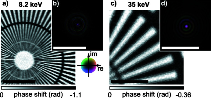
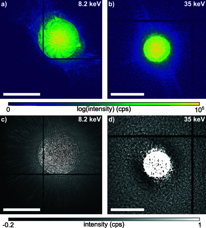
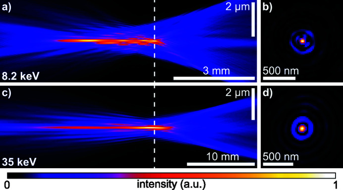
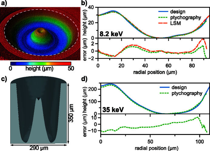
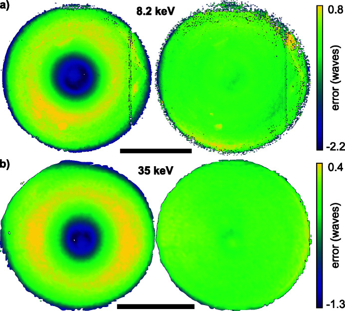
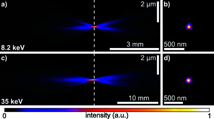
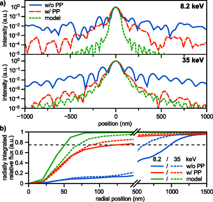
Modern subtractive and additive manufacturing techniques present new avenues for X-ray optics with complex shapes and patterns. Refractive phase plates acting as glasses for X-ray optics have been fabricated, and spherical aberration in refractive X-ray lenses made from beryllium has been successfully corrected. A diamond phase plate made by femtosecond laser ablation was found to improve the Strehl ratio of a lens stack with a numerical aperture (NA) of 0.88 × 10⁻³ at 8.2 keV from 0.1 to 0.7. A polymer phase plate made by additive printing achieved an increase in the Strehl ratio of a lens stack at 35 keV with NA of 0.18 × 10⁻³ from 0.15 to 0.89, demonstrating diffraction-limited nanofocusing at high X-ray energies.

Keywords: aberration correction; phase plate; ptychography; refractive X-ray optics.


Figures

Figure 1
Figure 1
Schematic of the beamline setup at both I13-1 of DLS and P06 of PETRA III. At I13-1 we used a stack of 50 Be CRLs at 8.2 keV with a total length of L CRL = 55 mm. At P06 we used 149 Be CRLs at 35 keV with a stack length of L CRL = 298 mm. All other distances can be found in Table 1 ▸.
Figure 2
Figure 2
Ptychographic reconstructions of the test objects and illuminating wavefields obtained at 8.2 keV (a, b) and 35 keV (c, d). (a) Reconstructed object phase shift of a Siemens star patterned into a 500 nm-thick gold layer. (b) Reconstructed complex illumination function in the object plane. Both images in (a) and (b) are shown at the same scale and the bar represents 4 µm. (c) Reconstructed object phase shift of a Siemens star patterned into a 500 nm-thick tantalum layer. (d) Reconstructed complex illumination function in the object plane. Both images in (c) and (d) are shown at the same scale and the bar represents 2 µm.
Figure 3
Figure 3
Example of diffraction patterns and average background signal, which is calculated from the difference between measured data and modeled diffraction patterns from ptychography. (a) Cropped diffraction pattern recorded with a Merlin detector at 8.2 keV. The beam is off-center as the detector ends in the upper right corner. (b) Cropped diffraction pattern at 35.0 keV recorded with the Lambda 2M GaAs detector. (c) Average background at 8.2 keV with the Merlin Si sensor. (d) Average background at 35 keV with the Lambda GaAs sensor. The scale bar in all images represents a scattering vector of 0.1 nm−1.
Figure 4
Figure 4
Characterized X-ray beams with spherical aberration. (a) Horizontal beam caustic at 8.2 keV. (b) Intensity distribution in the plane with highest peak intensity, marked by the dashed line in (a). (c) Horizontal beam caustic at 35 keV. (d) Intensity distribution in the plane with highest peak intensity, marked by the dashed line in (c).
Figure 5
Figure 5
Refractive phase plates and their thickness profiles. (a) Surface of the diamond phase plate used at 8.2 keV, acquired by a Keyence VK-X1100 laser scanning microsope (LSM). The dashed circle represents a diameter of 220 µm. The optically relevant region of the phase plate has a smaller diameter of only 186 µm. (b) Radial height profiles of the diamond phase plate shown in (a) measured via ptychography (green, dotted line) and LSM (orange, dashed line) in comparison with the design goal (blue, solid line). The error for both measurements against the design goal is shown in the lower subplot. (c) 3D rendering of the polymer phase plate used at 35 keV. The model is sliced in the middle for better visibility of the characteristic phase plate shape. (d) Radial height profile of the polymer phase plate shown in (c) measured via ptychography (green, dotted line) in comparison with the design goal (blue, solid line). The error against the design goal is shown in the lower subplot.
Figure 6
Figure 6
Residual wavefield error in the plane of the phase plate. (a) Wavefield error in the plane located 10.5 mm downstream of the lens exit aperture of 50 Be CRLs at 8.2 keV with (right) and without (left) corrective phase plate. (b) Wavefield error in the plane located 20 mm downstream of the lens exit aperture of 149 Be CRL at 35 keV with (right) and without (left) corrective phase plate. The scale bar in both figures represents 100 µm.
Figure 7
Figure 7
X-ray beams after correction with a phase plate as characterized by ptychography. (a) Horizontal beam caustic at 8.2 keV after correction with the diamond phase plate shown in Fig. 5 ▸(a). (b) Intensity distribution in the plane with highest peak intensity, marked by the dashed line in (a). (c) Horizontal beam caustic at 35 keV after correction with the polymer phase plate shown in Fig. 5 ▸(c). (d) Intensity distribution in the plane with highest peak intensity, marked by the dashed line in (c).
Figure 8
Figure 8
Intensity distribution in the focal plane. (a) Upper subplot: horizontal beam profile at 8.2 keV with the diamond phase plate (orange, dashed line) compared with the aberrated (blue, solid line) and ideal (green, dotted line) lens. Lower subplot: horizontal beam profile at 35 keV with the polymer phase plate (orange, dashed line) compared with the aberrated (blue, solid line) and ideal (green, dotted line) lens. (b) Radially integrated intensity distribution at both 8.2 keV (solid lines) and 35 keV (dotted lines), comparing the aberrated lens (blue) with the phase plate corrected (orange) and ideal (green) lens. The dashed horizontal line marks 0.75.
Figure 9
Figure 9
Resolution in scanning X-ray microscopy at 35 keV with corrective phase plate. (a) Reconstructed object phase shift via ptychography from the central part of a Siemens star test object. Spoke features range from 50 nm size in the innermost circle to about 200 nm for the outermost circle. (b) The same area as in (a), but in fluorescence contrast. The scan was performed with 100 nm steps with 21 × 21 scan points. The scale bar in both images represents 2 µm. The innermost spoke size in each radial segment is noted below the figures.

References

    1. Alianelli, L., Sawhney, K. J. S., Malik, A., Fox, O. J. L., May, P. W., Stevens, R., Loader, I. M. & Wilson, M. C. (2010). J. Appl. Phys. 108, 123107.
    1. Antipov, S., Assoufid, L., Grizolli, W., Qian, J. & Shi, X. (2018). Proceedings of the 9th International Particle Accelerator Conference (IPAC’18), 29 April–4 May 2018, Vancouver, BC, Canada, pp. 4057–4058. THPMF011.
    1. Bernert, C., Hoppe, R., Wittwer, F., Woike, T. & Schroer, C. G. (2017). Opt. Express, 25, 31640. - PubMed
    1. Celestre, R., Berujon, S., Roth, T., Sanchez del Rio, M. & Barrett, R. (2020). J. Synchrotron Rad. 27, 305–318. - PMC - PubMed
    1. Heimann, P., MacDonald, M., Nagler, B., Lee, H. J., Galtier, E., Arnold, B. & Xing, Z. (2016). J. Synchrotron Rad. 23, 425–429. - PMC - PubMed