Beam damage of single semiconductor nanowires during X-ray nanobeam diffraction experiments
- PMID: 32876594
- PMCID: PMC7467348
- DOI: 10.1107/S1600577520009789
Beam damage of single semiconductor nanowires during X-ray nanobeam diffraction experiments
Abstract
Nanoprobe X-ray diffraction (nXRD) using focused synchrotron radiation is a powerful technique to study the structural properties of individual semiconductor nanowires. However, when performing the experiment under ambient conditions, the required high X-ray dose and prolonged exposure times can lead to radiation damage. To unveil the origin of radiation damage, a comparison is made of nXRD experiments carried out on individual semiconductor nanowires in their as-grown geometry both under ambient conditions and under He atmosphere at the microfocus station of the P08 beamline at the third-generation source PETRA III. Using an incident X-ray beam energy of 9 keV and photon flux of 1010 s-1, the axial lattice parameter and tilt of individual GaAs/In0.2Ga0.8As/GaAs core-shell nanowires were monitored by continuously recording reciprocal-space maps of the 111 Bragg reflection at a fixed spatial position over several hours. In addition, the emission properties of the (In,Ga)As quantum well, the atomic composition of the exposed nanowires and the nanowire morphology were studied by cathodoluminescence spectroscopy, energy-dispersive X-ray spectroscopy and scanning electron microscopy, respectively, both prior to and after nXRD exposure. Nanowires exposed under ambient conditions show severe optical and morphological damage, which was reduced for nanowires exposed under He atmosphere. The observed damage can be largely attributed to an oxidation process from X-ray-induced ozone reactions in air. Due to the lower heat-transfer coefficient compared with GaAs, this oxide shell limits the heat transfer through the nanowire side facets, which is considered as the main channel of heat dissipation for nanowires in the as-grown geometry.
Keywords: air and He atmosphere; individual core–shell nanowires; morphological and optical changes; nanoprobe X-ray exposure; ozone-induced oxidation.
open access.
Figures


 ,
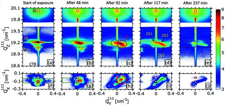
,  ) reciprocal-space plane for NW2 exposed in air. The two dashed curves in represent the ZB (top) and WZ (bottom) Debye–Scherrer rings. The red and pink dotted circles named P and T are explained in Fig. 1 ▸(e) and represent sub-Bragg peaks that originate from NW sections illuminated by the peak and tail of the Gaussian beam. The peaks named ZB1–ZB3 are referred to in Fig. 6 ▸(d). (f)–(j) 2D projections of the 111 Bragg reflection in the (,
  ) reciprocal-space plane. The red and black circles represent the positions of the Si CTR and the initial NW tilt, respectively, in and . The time at which each RSM acquisition was started is mentioned at the top.
 , ) reciprocal-space plane. The two dashed curves in represent the ZB (top) and WZ (bottom) Debye–Scherrer rings. (e)–(h) 2D projections of the 111 Bragg reflection in the (, ) reciprocal-space plane. The red and black circles represent the positions of the Si CTR and the initial NW tilt, respectively. The time at which each RSM acquisition was started is mentioned at the top.
 and , respectively. The blue hexagon represents the NW cross section and the black arrow represents the tilt direction. Red data points correspond to section P, whereas the pink ones correspond to section T of NW2. The black points correspond to NW4, exposed for 3 h under He atmosphere. (c) Intensity decay of the integrated 111 Bragg reflection for the two NWs. The red curve is an exponential fit. Error bars are within the size of the dots. (d) Variation in the c lattice parameter. The orange points correspond to the WZ reflection. The three ZB sub-peaks, colored in pink, were named ZB1–ZB3 as indicated in Fig. 4 ▸(d).
References
-
- Al Hassan, A., Davtyan, A., Küpers, H., Lewis, R. B., Bahrami, D., Bertram, F., Bussone, G., Richter, C., Geelhaar, L. & Pietsch, U. (2018b). J. Appl. Cryst. 51, 1387–1395.
-
- Al Hassan, A., Lewis, R. B., Küpers, H., Lin, W.-H., Bahrami, D., Krause, T., Salomon, D., Tahraoui, A., Hanke, M., Geelhaar, L. & Pietsch, U. (2018a). Phys. Rev. Mater. 2, 014604.
-
- Biermanns, A., Rieger, T., Bussone, G., Pietsch, U., Grützmacher, D. & Ion Lepsa, M. (2013). Appl. Phys. Lett. 102, 043109.
-
- Boller, K., Haelbich, R.-P., Hogrefe, H., Jark, W. & Kunz, C. (1983). Nucl. Instrum. Methods Phys. Res. 208, 273–279.
-
- Claeys, C. & Simoen, E. (2002). Radiation Effects in Advanced Semiconductor Materials and Devices, Vol. 57, pp. 245–280. Springer Series in Materials Science. Berlin, Heidelberg: Springer-Verlag.
Grants and funding
LinkOut - more resources
Full Text Sources
Research Materials