. 2020 Sep 2;11(1):4406.
doi: 10.1038/s41467-020-18195-0.

Stochastic resonance in MoS2 photodetector

Affiliations

Stochastic resonance in MoS2 photodetector

Akhil Dodda et al. Nat Commun. .

Abstract

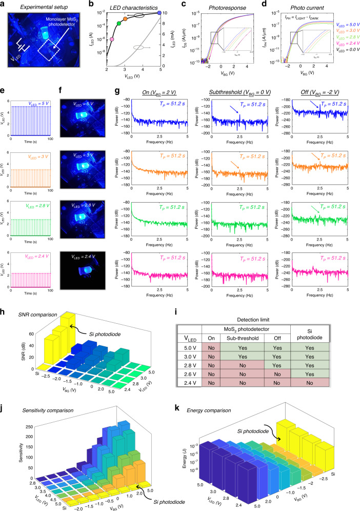
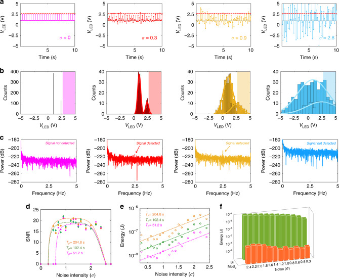
In this article, we adopt a radical approach for next generation ultra-low-power sensor design by embracing the evolutionary success of animals with extraordinary sensory information processing capabilities that allow them to survive in extreme and resource constrained environments. Stochastic resonance (SR) is one of those astounding phenomena, where noise, which is considered detrimental for electronic circuits and communication systems, plays a constructive role in the detection of weak signals. Here, we show SR in a photodetector based on monolayer MoS2 for detecting ultra-low-intensity subthreshold optical signals from a distant light emitting diode (LED). We demonstrate that weak periodic LED signals, which are otherwise undetectable, can be detected by a MoS2 photodetector in the presence of a finite and optimum amount of white Gaussian noise at a frugal energy expenditure of few tens of nano-Joules. The concept of SR is generic in nature and can be extended beyond photodetector to any other sensors.


Conflict of interest statement

The authors declare no competing interests.

Figures

Fig. 1
Fig. 1. Monolayer MoS2 synthesis, characterization, and device fabrication.
a Schematic of cold-wall horizontal reactor setup. b Coalesced monolayer MoS2 film grown on a 2-inch sapphire substrate using MOCVD at 1000 °C with Mo(CO)6 and H2S as precursors. c AFM images at the center and edge of the wafer showing uniform surface coverage, film morphology, and thickness. d In-plane X-ray diffraction showing the epitaxial relation between MoS2 and sapphire as (101¯0) MoS2 ‖ (101¯0) α-Al2O3. The inset shows a narrow full-width half-maximum (FWHM) of 0.27°, which emphasizes the high crystalline quality of these monolayer films. Raman map of (e) E2g1 and (f) A1g peaks show <5% variation and the peak separation of 18 cm−1 confirms monolayer MoS2. g Photoluminescence (PL) map shows an intense peak at 1.84 eV, which is attributed to the indirect to direct bandgap transition in monolayers and is severely suppressed in multilayers of MoS2. h Schematic and i SEM image of monolayer MoS2 FET. j Logarithmic scale and k linear scale transfer characteristics of monolayer MoS2 FET measured at different drain biases (VD). l Mobility plot and m output characteristics measured at different back gate biases (VBG).
Fig. 2
Fig. 2. Demonstration of stochastic resonance (SR) in monolayer MoS2 field-effect transistor (FET).
a Schematic showing the basic concept of SR with three essential components: a nonlinear thresholding device, a weak coherent input such as a periodic signal, and a source of noise. When the noise intensity reaches some finite and appropriate level, the system can detect the weak time-variant signal, which otherwise lies below the detection threshold of the sensor. b A 2.5 Hz square wave of amplitude 0.4 V is applied to the back-gate of the monolayer MoS2 FET at different operating regimes: ON-state (VBG = 3.5 V), subthreshold (VBG = −1 V), and OFF-state (VBG = −2.5 V). c Output current (IDS) and d corresponding PSD plots obtained using the FFT. Current sampling was done at 20 Hz for ~100 s. In the ON-state and subthreshold regime the signal is detected, whereas, in the OFF-state, IDS is obscured by the noise floor and corresponding peaks are absent in the PSD. e In order to detect the signal in the OFF-state, Gaussian noise of different standard deviations (σ) are superimposed on the square wave centered at VBG = −2.5 V. f PSD of measured IDS. The current sampling was done at 20 Hz for ~400 s. The signal is detected for an optimum amount of Gaussian noise, confirming SR in MoS2 FET. g SNR as a function of σ for various total sampling time (TP). h Color map of the correlation coefficient (CC) between IDS and VBG. i Energy consumption as a function of σ for various TP. Clearly, optimum signal detection can be achieved with energy as frugal as 10–100 nJ corresponding to σ = 0.5 V.
Fig. 3
Fig. 3. Detection limit of monolayer MoS2 photodetector.
a Experimental setup showing the photodetector chip based on monolayer MoS2 FET placed at a distance of ~1 cm from a blue LED. b Current (ILED) versus voltage (VLED) characteristics of the LED. c Transfer characteristics of the MoS2 FET under dark and illumination corresponding to different VLEG. d The extracted photocurrents (IPH). e 2.5 Hz periodic signals of different amplitudes applied to the LED and f corresponding snapshots of the glowing LED. The LED intensity drops linearly for 5 V > VLED > 2.8 V and exponentially for VLED < 2.8 V in accordance with the output characteristics of the LED, as indicated using the colored circles in (b). g PSD plots obtained from FFT of IDS for a total duration of TP = 51.2 s in different operation regimes in response to periodic LED signals in (e). Peaks observed in the PSD at 2.5 Hz are indications of successful detection of the LED signal. h Extracted SNR in different detection regimes for various LED illuminations. For comparison, we have also included the results obtained from the same experiments performed on a commercial Si photodiode in Supplementary Note 6. i Table summarizing the detection limit for the blue light by MoS2 photodetector and Si photodiode. j Sensitivity of the MoS2 photodetector in different detection regimes. The sensitivity (S) of a photodetector is defined as the ratio of photocurrent (IPH) to the luminous flux (Lϕ). The rated sensitivity of the Si photodiode (S = 9 nA/lx) and its photoresponse to different VLED were used for calibrating Lϕ, which were subsequently used to calculate the sensitivity of MoS2 photodetector. k Comparison of energy expenditure for the Si photodiode and MoS2 photodetector for detection of above threshold signals. The MoS2 photodetector offers orders of magnitude higher energy efficiency when operated in the subthreshold regime, owing to significantly lower dark current.
Fig. 4
Fig. 4. Demonstration of SR in monolayer MoS2 photodetector.
a White Gaussian noise of different standard deviations (σ) superimposed on 2.5 Hz periodic and subthreshold LED signal of amplitude VLED = 2.4 V and b corresponding histogram of the LED voltage distribution. Each histogram shows two Gaussian curves of the same variance but different means, one centered at VLED = 1 V (LED OFF) and the other one centered at VLED = 2.4 V (Dim LED), marking the level difference between the two states of the LED signal. c PSD plots obtained from the FFT of the output current (IDS) measured in the monolayer MoS2 photodetector for a total duration of TP = 204.8 s in response to the LED signals in (a). The MoS2 photodetector was biased in the OFF-state (VBG = −2 V). In the presence of a finite and appropriate amount of noise, the subthreshold LED signal is detected. (see Supplementary video files 1–3 for real-time observation of SR in the MoS2 photodetector). d SNR as a function of σ for different sampling time TP. For very low variance Gaussian noise (σ < 0.2 V), the signal hardly crosses the detection threshold of the MoS2 photodetector, i.e., VLED = 2.6 V. As σ increases, a larger fraction of the LED signal corresponding to the 2.4 V level crosses the detection threshold of the MoS2 photodetector, increasing the SNR. For even larger variances, the SNR starts to decrease since the tail of the Gaussian distribution centered at VLED = 1 V will also start to cross the detection threshold of the MoS2 photodetector, obscuring the periodicity of the VLED = 2.4 V signal. The SNR curves in this instance show the typical SR response found in biological species such as paddlefish, crayfish, etc. e Energy consumption by the MoS2 photodetector is plotted as a function of σ for different TP. Since the MoS2 photodetector was operated in the deep OFF-state (VBG = −2 V) to minimize the dark current, the operating power budget is drastically reduced, making the signal detection extremely energy efficient. For comparison, refer to Supplementary Note 9 for the exploitation  of SR using the Si photodiode (see Supplementary video files 4–6 for real-time observation of SR in the Si photodiode). f The energy consumption by the Si photodiode for detecting subthreshold optical signal, exploiting SR, is found to be in the range of a few micro-Joules, which is 1000X higher compared to the MoS2 photodetector for sampling time TP = 100 s.

References

    1. Wiesenfeld K, Moss F. Stochastic resonance and the benefits of noise: from ice ages to crayfish and SQUIDs. Nature. 1995;373:33. - PubMed
    1. Nicolis C. Long-term climatic transitions and stochastic resonance. J. Stat. Phys. 1993;70:3–14.
    1. Benzi R, Sutera A, Vulpiani A. The mechanism of stochastic resonance. J. Phys. A: Math. Gen. 1981;14:L453.
    1. Douglass JK, Wilkens L, Pantazelou E, Moss F. Noise enhancement of information transfer in crayfish mechanoreceptors by stochastic resonance. Nature. 1993;365:337. - PubMed
    1. Russell DF, Wilkens LA, Moss F. Use of behavioural stochastic resonance by paddle fish for feeding. Nature. 1999;402:291. - PubMed

Publication types