. 2020 Sep 7;11(1):4442.
doi: 10.1038/s41467-020-18307-w.

Room temperature near unity spin polarization in 2D Van der Waals heterostructures

Affiliations

Room temperature near unity spin polarization in 2D Van der Waals heterostructures

Danliang Zhang et al. Nat Commun. .

Abstract

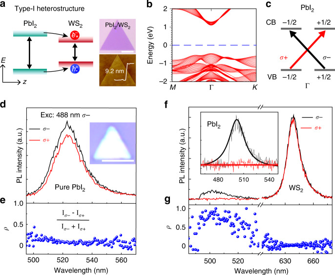
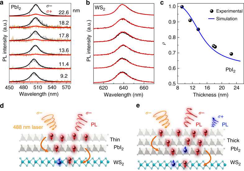
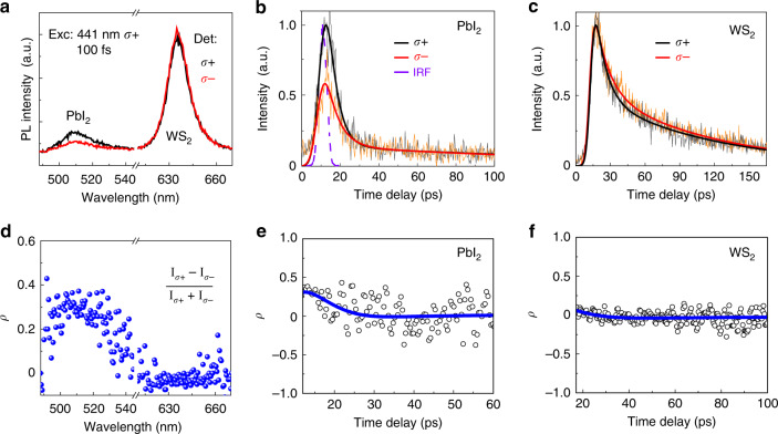
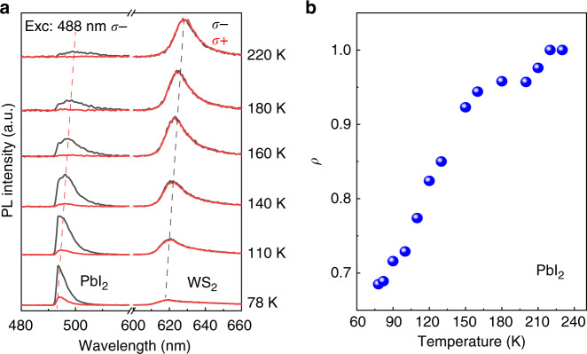
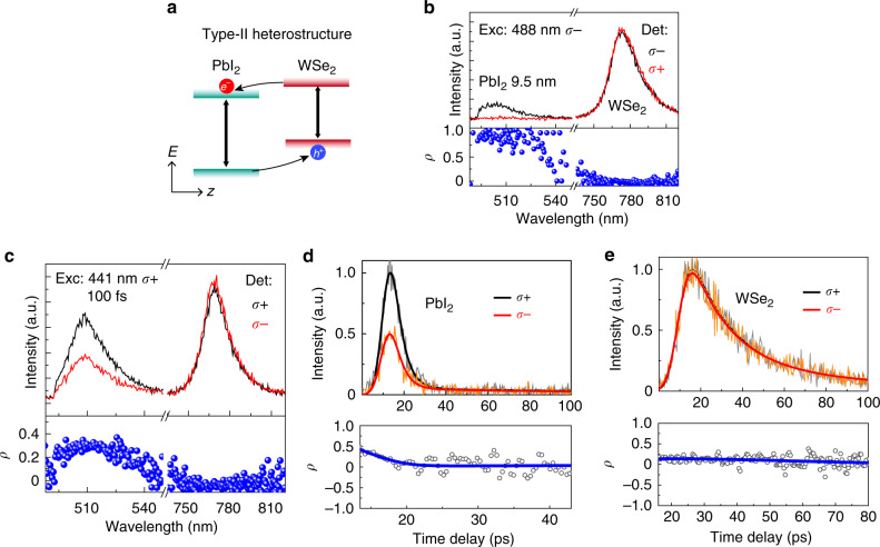
The generation and manipulation of spin polarization at room temperature are essential for 2D van der Waals (vdW) materials-based spin-photonic and spintronic applications. However, most of the high degree polarization is achieved at cryogenic temperatures, where the spin-valley polarization lifetime is increased. Here, we report on room temperature high-spin polarization in 2D layers by reducing its carrier lifetime via the construction of vdW heterostructures. A near unity degree of polarization is observed in PbI2 layers with the formation of type-I and type-II band aligned vdW heterostructures with monolayer WS2 and WSe2. We demonstrate that the spin polarization is related to the carrier lifetime and can be manipulated by the layer thickness, temperature, and excitation wavelength. We further elucidate the carrier dynamics and measure the polarization lifetime in these heterostructures. Our work provides a promising approach to achieve room temperature high-spin polarizations, which contribute to spin-photonics applications.


Conflict of interest statement

The authors declare no competing interests.

Figures

Fig. 1
Fig. 1. Spin polarization mechanism and spectrum of PbI2/WS2 heterostructures.
a Schematic of the type-I heterostructure for the study of the carrier interlayer transportation. Both electrons and holes transfer from PbI2 to WS2. The images on the right are optical and AFM micrographs of a PbI2/WS2 heterostructure with a thickness of 9.2 nm. b Band structure for the PbI2 thin film with a thickness of 20 layers, which is spin degenerate. c Schematic illustration of the polarized optical transitions in PbI2 thin films. d Circularly polarized PL spectra from pure PbI2 at room temperature. e Corresponding degree of polarization ρ of pure PbI2 PL calculated from the PL spectra shown in figure (d). f Circularly polarized PL spectra of a representative PbI2/WS2 heterostructure at room temperature. g Corresponding degree of polarization ρ calculated from the PL spectra shown in figure (f). All length of the scale bar is 10 µm.
Fig. 2
Fig. 2. Thickness-dependent spin polarization and the underlying mechanism in PbI2/WS2 heterostructures.
a, b Circularly polarized PL spectra of PbI2 and WS2 in PbI2/WS2 heterostructures with different thicknesses. c Degree of polarization ρ of PbI2 as a function of thickness of the heterostructures. The solid line represents the numerical simulation result. d, e Schematic illustrations of the resulting spin polarization in the thin and thick PbI2/WS2 heterostructures. The curled curves represent the incident light and the PL emissions. The red balls represent spin-down electrons, and the blue balls represent spin-up electrons.
Fig. 3
Fig. 3. Spin polarization dynamics of PbI2/WS2 heterostructures.
ac Circularly polarized PL spectra (a) and TRPL data from PbI2 (b), and WS2 (c) of PbI2/WS2 heterostructures. df Corresponding degree of polarization ρ as a function of wavelength and time calculated from the PL and TRPL spectra. For excitation, a 441 nm σ+ polarized fs-pulsed laser beam was used.
Fig. 4
Fig. 4. Temperature-dependent degree of polarization from PbI2/WS2 heterostructures.
a Circularly polarized PL spectra of PbI2/WS2 heterostructure at different temperatures for excitation with a 488 nm σ− polarized CW laser beam. b Degree of polarization ρ of PL from PbI2 as a function of temperature, showing a decreasing tendency at lower temperatures.
Fig. 5
Fig. 5. Degree of spin polarization and the dynamics in PbI2/WSe2 heterostructures.
a Schematic of the type-II band alignment and the corresponding photogenerated carrier behaviors in PbI2/WSe2 heterostructures. b Circularly polarized PL spectra from a 9.5 nm thick PbI2/WSe2 heterostructure, and the corresponding calculated ρ as a function of wavelength. The excitation is 488 nm σ− polarized CW laser. ce Circularly polarized PL spectra (c) and TRPL data from PbI2 (d) and WSe2 (e) in PbI2/WSe2 heterostructure, and the corresponding degree of polarization ρ calculated from PL and TRPL spectra. Excitation with 441 nm σ+ polarization femtosecond laser pulses.

References

    1. Geim AK, Grigorieva IV. Van der Waals Heterostructures. Nature. 2013;499:419–425. - PubMed
    1. Liu Y, et al. Van der Waals heterostructures and devices. Nat. Rev. Mater. 2016;1:16042.
    1. Jariwala D, Marks TJ, Hersam MC. Mixed-dimensional van der Waals heterostructures. Nat. Mater. 2017;16:170–181. - PubMed
    1. Wang QH, Kalantar-Zadeh K, Kis A, Coleman JN, Strano MS. Electronics and optoelectronics of two-dimensional transition metal dichalcogenides. Nat. Nanotechnol. 2012;7:699–712. - PubMed
    1. Mak KF, Shan J. Photonics and optoelectronics of 2D semiconductor transition metal dichalcogenides. Nat. Photon. 2016;10:216–226.