. 2020 Sep 2;6(36):eabb6500.
doi: 10.1126/sciadv.abb6500. Print 2020 Sep.

Anisotropic ultrasensitive PdTe2-based phototransistor for room-temperature long-wavelength detection

Affiliations

Anisotropic ultrasensitive PdTe2-based phototransistor for room-temperature long-wavelength detection

Cheng Guo et al. Sci Adv. .

Abstract

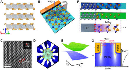
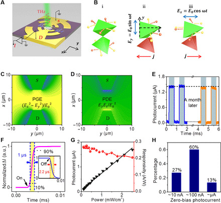
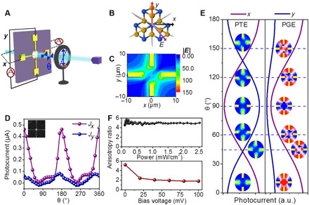
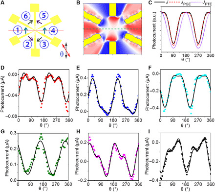
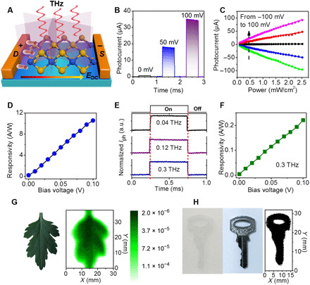
Emergent topological Dirac semimetals afford fresh pathways for optoelectronics, although device implementation has been elusive to date. Specifically, palladium ditelluride (PdTe2) combines the capabilities provided by its peculiar band structure, with topologically protected electronic states, with advantages related to the occurrence of high-mobility charge carriers and ambient stability. Here, we demonstrate large photogalvanic effects with high anisotropy at terahertz frequency in PdTe2-based devices. A responsivity of 10 A/W and a noise-equivalent power lower than 2 pW/Hz0.5 are achieved at room temperature, validating the suitability of PdTe2-based devices for applications in photosensing, polarization-sensitive detection, and large-area fast imaging. Our findings open opportunities for exploring uncooled and sensitive photoelectronic devices based on topological semimetals, especially in the highly pursuit terahertz band.


Figures

Fig. 1
Fig. 1. Characterization and interface behavior of type II DSM PdTe2.
(A) Crystallographic structure of PdTe2. Orange and blue balls denote Te and Pd atoms, respectively. (B) Microscopic view of the metal-PdTe2 contact along with the atomic chains. The shaded area represents the mirror planes on the (001) surface. (C) HR-TEM images of PdTe2 single crystal. (D) The coexistence of hole and electron pockets in the Fermi surface along the kx-ky plane as a result of the type II Dirac cone. The hole pocket was marked by the red dotted circle, whereas the electron pocket, corresponding to the translucent aqua-like pocket, forms an apple pit–shaped pocket in the reciprocal space. (E) The projection of the Dirac cone along the kx-kz plane. The tilted Dirac cone is evident along the kz direction. (F) The charge density (top) and charge density difference (middle) near the metal (Cr/Au)–PdTe2 interface. The bottom panel represents a schematic diagram of the corresponding range of atomic structures. (G) The cross-sectional view of localized-field distribution along the c axis near the metal-PdTe2 interface under terahertz illumination.
Fig. 2
Fig. 2. The photoresponse of unbiased PdTe2-based devices at 300 K.
(A) Schematic diagram of the PdTe2-based photodetector. (B) The process of the PGE and its dependence on the polarized terahertz field. (i) Carrier scattering from scatters without terahertz field. (ii and iii) Ratchet scatterings under action of terahertz field with y and x polarizations. (C and D) The contributions of PGE and PDE in a single device under 0.48-meV terahertz excitation. (E) The impulse photocurrent response of the PdTe2-based device after exposure to ambient atmosphere for 1 month (hυ ~ 0.48 meV and power density ~ 2.5 mW/cm2). (F) Display of rising and falling edges of the time-resolved response in a single period, exhibiting the video-rate time response at around 1 and 2.2 μs. a.u., arbitrary units. (G) Dependence of the photocurrent (black solid symbols, left axis) and the responsivity (red symbols, right axis) on the radiation power intensity. (H) The counts of unbiased devices with different magnitudes of photocurrent.
Fig. 3
Fig. 3. The anisotropic photocurrent of the PdTe2-based device at zero-bias voltage.
(A) Schematic diagram of the polarization-resolved photocurrent measurement setup. (B) Ideal microscopic diagram of polarization field and relative direction of material. (C) Simulated electric field distribution at specific polarization angle (45°). (D) Dependence of the photocurrents (Jx, Jy) along two orthogonal axes on the polarization angle θ (inset: scanning electron microscope image of the four-terminal PdTe2-based device). (E) Comparison of theoretical results of PGE and PTE in x and y directions. (F) Relationship between anisotropic ratio (Jx/Jy) and incident power (top) and bias (bottom).
Fig. 4
Fig. 4. Polarization-resolved photocurrent in a circularly arranged contact device.
(A) Schematic diagram of the experimental setup for polarization-resolved photocurrent measurement. The photocurrent was collected between nearest electrode pairs around the sample in the sequence of anticlockwise. θ is the angle of incident light polarization. (B) Simulated distribution of PGE photocurrent at θ = 45° (see fig. S5 for additional angular configurations). (C) Dependence of the photocurrent on polarization angle θ. JPGE derives from PGE, and JPTE is related to PTE. J = Asin(4θ + a) + Bcos(2θ + b) + C. (D to I) Dependence of the photocurrent on different electrode pairs (① to ⑥) on polarization angle θ.
Fig. 5
Fig. 5. The photoresponse of the biased PdTe2-based device and its noninvasive imaging applications.
(A) Schematic diagram of the measurement of the bias-mode photocurrent mechanism. (B) The time-resolved photocurrent response of the device in a single period (1 ms) at different bias voltages with a light source at 0.12 THz and a power density of 0.525 mW/cm2. (C) Dependence of the photocurrent on the radiation power intensity at different bias voltages. (D) Dependence of the responsivity on the bias voltage. (E) The time-resolved photoresponse at different photon frequencies. (F) Dependence of the responsivity on the bias voltage at 0.3 THz. (G and H) The terahertz imaging of a fresh leaf (0.12 THz) and the hidden key (0.3 THz) at 300 K. Photo credit: Cheng Guo, State Key Laboratory for Infrared Physics, Shanghai Institute of Technical Physics, Chinese Academy of Sciences.

References

    1. Tang F., Po H. C., Vishwanath A., Wan X., Comprehensive search for topological materials using symmetry indicators. Nature 566, 486–489 (2019). - PubMed
    1. Liu D. F., Liang A. J., Liu E. K., Xu Q. N., Li Y. W., Chen C., Pei D., Shi W. J., Mo S. K., Dudin P., Kim T., Cacho C., Li G., Sun Y., Yang L. X., Liu Z. K., Parkin S. S. P., Felser C., Chen Y. L., Magnetic Weyl semimetal phase in a Kagome crystal. Science 365, 1282–1285 (2019). - PubMed
    1. Clark O. J., Neat M. J., Okawa K., Bawden L., Marković I., Mazzola F., Feng J., Sunko V., Riley J. M., Meevasana W., Fujii J., Vobornik I., Kim T. K., Hoesch M., Sasagawa T., Wahl P., Bahramy M. S., King P. D. C., Fermiology and superconductivity of topological surface states in PdTe2. Phys. Rev. Lett. 120, 156401 (2018). - PubMed
    1. Sajadi E., Palomaki T., Fei Z., Zhao W., Bement P., Olsen C., Luescher S., Xu X., Folk J. A., Cobden D. H., Gate-induced superconductivity in a monolayer topological insulator. Science 362, 922–925 (2018). - PubMed
    1. Li J. H., Li Y., Du S. Q., Wang Z., Gu B. L., Zhang S. C., He K., Duan W. H., Xu Y., Intrinsic magnetic topological insulators in van der Waals layered MnBi2Te4-family materials. Sci. Adv. 5, eaaw5685 (2019). - PMC - PubMed

LinkOut - more resources