

Quantitative SEM characterisation of ceramic target prior and after magnetron sputtering: a case study of aluminium zinc oxide
- PMID: 32926411
- PMCID: PMC7891359
- DOI: 10.1111/jmi.12961
Quantitative SEM characterisation of ceramic target prior and after magnetron sputtering: a case study of aluminium zinc oxide
Abstract
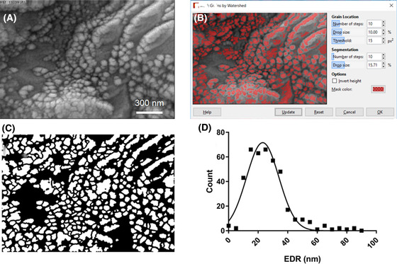
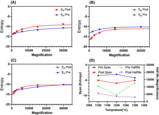
Till now electron microscopy techniques have not been used to evaluate the plasma-target interactions undergone during the magnetron sputtering process. The destructive nature of this interaction severely alters the target microstructure. Utilising quantitative microscopy techniques can shed light on the complex plasma and solid-state processes involved which can ultimately lead to improved functional thin film deposition. As a representative functional material, aluminium-doped-zinc oxide (AZO) is an upcoming alternative to conventional transparent electrode wherein the process optimisation is of great importance. In this paper, we evaluate the pre- and post-sputter field emission scanning electron microscopy (FESEM) data for ceramic AZO target fabricated at three final sintering temperatures (1100°C, 1200°C and 1300°C). In all cases, grain boundaries are merged in addition to a visible reduction in the secondary phases which makes segmentation-based image analysis challenging. Through surface statistics (i.e. fractal dimension, autocorrelation length, texture aspect ratio and entropy) as a function of magnification we can quantify the electron microscopy image of the microstructure. We show that the plasma-microstructure interaction leads to an increase in autocorrelation length, texture aspect ratio and entropy for the optimum AZO ceramic sputtering target sintered at 1200°C. Furthermore, a maximum reduction in fractal dimension span (as determined by exponential regression) is also observed for 1200°C. In addition to the evaluation of plasma effects on sintering, our approach can provide a window towards understanding the underlying thin film growth mechanisms. We believe that this technique can be applied to the defect characterisation of a wide range of polycrystalline ceramic sputtering targets (e.g. ITO, CZTS, GAZO and so on) with the ultimate goal of improving the magnetron sputtering process and the resulting functional thin film. LAY DESCRIPTION: Magnetron sputtering allows scientists to make functional thin films on the order of the nanoscale. In this technique, atoms are plucked from a 'target' then placed onto a substrate forming a thin nanometric film: all thanks to magnets, a special power supply and the fourth state of matter (plasma). Understanding what is going on and how to make a 'good' thin film is important for making better light emitting diodes, solar cells and light sensors. Scientists use electron microscopy to see what is going on in the microstructure of the sputtered thin films to fine tune the sputtering recipe. Here, for the first time, we have applied electron microscopy to see the surface of the microstructure before and after magnetron sputtering. This will help us understanding the plasma-microstructure interaction allowing us to make more informed decisions when fine-tuning the sputtering process to get improved thin films. This is a case study of aluminium-doped zinc oxide (AZO) target that could potentially replace indium tin oxide (ITO), which is widely used as a transparent electrode in devices involving light and electricity. In this case, improved characteristics would be lower electrical resistivity and higher transmission of light. We show that it is possible to use a mathematical description (e.g. the fractal dimension) of the scanning electron microscopy picture to show a link between the target surface and the functional properties. Simple explanation of fractal dimensions by Sixty Symbols ○ https://www.youtube.com/watch?v=cmBljeC79Ls Experimental demonstration of magnetron sputtering by The Thought Emporium ○ https://www.youtube.com/watch?v=Cyu7etM-0Ko Introductory video on magnetron sputtering by Applied Science ○ https://www.youtube.com/watch?v=9OEz_e9C4KM Demonstration of AZO target fabrication and sputtering by Pradhyut Rajjkumar ○ https://www.youtube.com/watch?v=kTLaTJfNX3c Simple explanation of a DIY SEM by Applied Science ○ https://www.youtube.com/watch?v=VdjYVF4a6iU.
Keywords: Aluminium-doped zinc oxide (AZO); field-emission scanning electron microscopy (FESEM); image processing; magnetron sputtering; microstructure characterisation; plasma.
© 2020 The Authors. Journal of Microscopy published by John Wiley & Sons Ltd on behalf of Royal Microscopical Society.
Conflict of interest statement
The authors report no conflict of interests. The authors alone are responsible for the content and writing of the paper.
Figures


References
-
- Barber, V.C. & Emerson, C.J. (1979) Techniques utilizing real time stereo scanning electron microscopy in the microdissection of biological tissues. J. Microsc. 115, 119–125. - PubMed
-
- Bose, S. , Arokiyadoss, R. , Bhargav, P.B. , Ahmad, G. , Mandal, S. , Barua, A.K. & Mukhopadhyay, S. (2018) Modification of surface morphology of sputtered AZO films with the variation of the oxygen. Mater. Sci. Semicond. Process. 79, 135–143.
-
- Brown, A.T. , Poon, W.C.K. , Holm, C. & de Graaf, J. (2017) Ionic screening and dissociation are crucial for understanding chemical self‐propulsion in polar solvents. Soft Matter 13, 1200–1222. - PubMed
-
- Castro, R.H.R. & van Benthem, K. (Eds.) (2013) Sintering: Mechanisms of Convention Nanodensification and Field Assisted Processes, Engineering Materials. Springer, Berlin, New York.
LinkOut - more resources
Full Text Sources
Research Materials
