Review
. 2020 Sep 12;20(18):5214.
doi: 10.3390/s20185214.

A Review of Piezoelectric PVDF Film by Electrospinning and Its Applications

Affiliations
Review

A Review of Piezoelectric PVDF Film by Electrospinning and Its Applications

Gulnur Kalimuldina et al. Sensors (Basel). .

Abstract

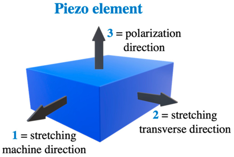
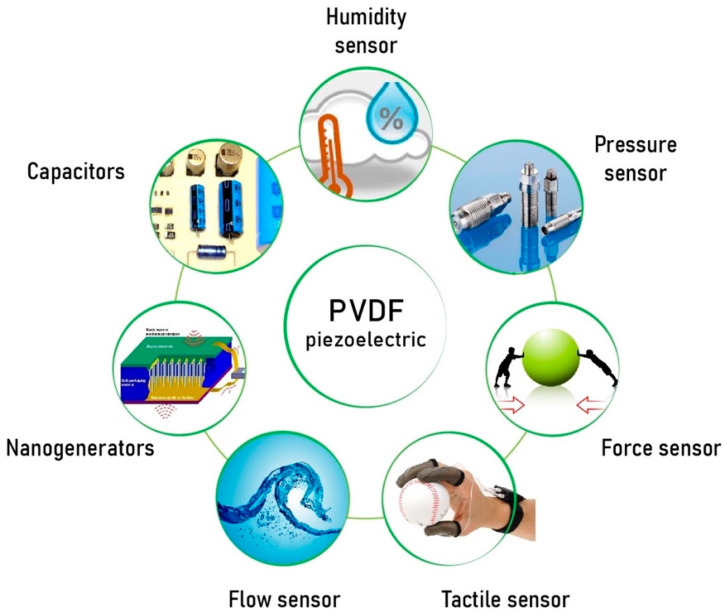
With the increase of interest in the application of piezoelectric polyvinylidene fluoride (PVDF) in nanogenerators (NGs), sensors, and microdevices, the most efficient and suitable methods of their synthesis are being pursued. Electrospinning is an effective method to prepare higher content β-phase PVDF nanofiber films without additional high voltage poling or mechanical stretching, and thus, it is considered an economically viable and relatively simple method. This work discusses the parameters affecting the preparation of the desired phase of the PVDF film with a higher electrical output. The design and selection of optimum preparation conditions such as solution concentration, solvents, the molecular weight of PVDF, and others lead to electrical properties and performance enhancement in the NG, sensor, and other applications. Additionally, the effect of the nanoparticle additives that showed efficient improvements in the PVDF films was discussed as well. For instance, additives of BaTiO3, carbon nanotubes, graphene, nanoclays, and others are summarized to show their contributions to the higher piezo response in the electrospun PVDF. The recently reported applications of electrospun PVDF films are also analyzed in this review paper.

Keywords: PENG; PVDF; PVDF nanofibers; electrospinning; nanogenerator; piezoelectricity; self-charging; sensors.


Conflict of interest statement

The authors declare no conflict of interest.

Figures

Figure 1
Figure 1
The main phases of polyvinylidene fluoride (PVDF) and β-PVDF induced by stretching and high voltage poling voltage.
Figure 2
Figure 2
Axis definition of piezo element.
Figure 3
Figure 3
Electrospinning/electrospraying setup. Reprinted with permission from [26].
Figure 4
Figure 4
Variation of electrospun membrane morphology with polymer concentration. Original magnification: 500× (left) and 10 k× (right). Voltage: 5 kV; flow rate: 0.3 mL/h; distance: 10 cm; DMF/acetone = 8/2. (a) 10%, (b) 13%, (c) 15%, (d) 17%, (e) 20% Reprinted with permission from [67].
Figure 5
Figure 5
Calculated fractions of β-phase of the above electrospun membranes as a function of mixed solvents with the different “X”/acetone volume ratios for the corresponding 16 wt.% PVDF solutions. The “X” stands for the fraction of one of the four solvents. Reprinted with permission from [73].
Figure 6
Figure 6
SEM images of aligned wrinkled electrospun PVDF fibers and their cross-section fabricated at different molecular weights. (a,d) Mw = 180 × 103. (b,e) Mw = 275 × 103. (c,f) Mw = 530 × 103. Reprinted with permission from [77].
Figure 7
Figure 7
Representative pictures of samples fabricated by electrospinning of PVDF solutions with different morphologies. (ac) Randomly oriented fibers, (a) wrinkled, (b) smooth, and (c) porous. (df) Aligned fibers, (d) wrinkled, (e) smooth, and (f) porous. Reprinted with permission from [78].
Figure 8
Figure 8
FE-SEM images of electrospun PVDF nanofibers prepared at ambient temperatures at (a) 5 °C, (b) 15 °C, (c) 25 °C, (d) 35 °C, (e) 45 °C. Reprinted with permission from [95].
Figure 9
Figure 9
Cross-sectional SEM images of samples fabricated by electrospinning 35% (w/v) PVDF solution from DMF at different levels of relative humidity (A) 5%, (B) 25%, (C) 45%, and (D) 65%. Reprinted with permission from [96].
Figure 10
Figure 10
(A) SEM and (B) TEM micrographs of Sample 2. It is evident that the BaTiO3 fiber is embedded within the PVDF matrix and aligned along its fiber axis. Reprinted with permission from [64].
Figure 11
Figure 11
The mechanism diagram of β-phase formation on barium titanate (BT) nanoparticles and graphene nanosheets in the nanocomposite fiber. Reprinted with permission from [107].
Figure 12
Figure 12
Schematic scheme of fabrication and application of the experimental procedure for β-PVDF-based nanogenerator. Reprinted with permission from [111].
Figure 13
Figure 13
SEM images of electrospun composite nanofibers of PVDF/nanoclay with different nanoclay contents: (a) 0.0 wt.% (pure PVDF); (b) 0.2 wt.% STN; (c) 1.0 wt.% STN; (d) 5.0 wt.% STN; (e) 10.0 wt.% STN; (f) 1.0 wt.% SWN; (g) 10.0 wt.% SWN. Electrospinning voltage is 20 kV and source-to-collector distance is 10 cm. The scale bar represents 2 microns. Reprinted with permission from [113].
Figure 14
Figure 14
(a) The volume and surface conductivities of polyvinylidene fluoride (PVDF)/multiwalled-carbon nanotubes (MWCNTs) nanofiber mats for different concentrations of MWCNTs dosages; (b) schematic diagram of PVDF/MWCNTs nanogenerator without stress; (c) working schematic of the PVDF-3% CNTs and PVDF-5% CNTs nanogenerators under stress; (d) working schematic of the PVDF-7% CNTs and PVDF-10% CNTs nanogenerators under stress. Reprinted with permission from [119].
Figure 15
Figure 15
FE-SEM micrographs of the dried electrospun PVDF fibers (a) without Al (NO3)3·9H2O, (b) with 8 wt.% Al (NO3)3·9H2O, and (c) with 16 wt.% Al (NO3)3·9H2O. Reprinted with permission from [123].
Figure 16
Figure 16
Applications of piezoelectric electrospun PVDF films for different devices.
Figure 17
Figure 17
The optical image (a) and the output voltages (b) generated by finger pressing-releasing process. A commercial electric watch and 15 LEDs driven by the converted electric energy from finger pressing-releasing process (c). The optical image and output voltages generated by human motions of (d) wrist bending, (e) finger taping and foot stepping by (f) heel and (g) toe. Reprinted with permission from [107].
Figure 18
Figure 18
(1) Structure diagram of wrist PVDF sensor; (2) Measured response waveforms of the sensor during different hand movements including (a) making a fist; (b) thumb bending; (c) wrist stretching and bending; and (d) wrist waving. Reprinted with permission from [37].
Figure 19
Figure 19
Schematic associated with the preparation of PVDF nanofibers (NFs), PVDF NFs-AgNPs electrodes and fabrication of piezoelectric sensor. Reprinted with permission from [134].
Figure 20
Figure 20
Modeling and meshing of fluid domain. Reprinted with permission from [135].
Figure 21
Figure 21
Wearable sensor for finger pressure sensing: (a) The diagram of sensor network attached on the hand. (b,c) The measured capacitance changes when a single and double pressure applied on the sensor network. (d) Plots showing the relative changes in capacitance of the sensor when it was subjected to dynamic pressing and releasing cycles. Reprinted with permission from [140].
Figure 22
Figure 22
Schematic representation of steps involved in the fabrication of siloxene self-charging supercapacitor power cells (SCSPC). (a) represents the preparation of siloxene sheets via topochemical deintercalation of calcium from CaSi2 in the presence of ice-cold HCl solution, (b) represents the fabrication process involved in the electrospinning of siloxene/PVDF piezo fibers, and (c) indicates the fabrication of a siloxene SCSPC device using siloxene sheets-coated carbon cloth as two symmetric electrodes and electrospun siloxene–PVDF piezo fibers impregnated with ionogel electrolyte as the separator. Reprinted with permission from [156].
Figure 23
Figure 23
Schematic illustration of the self-powered patterned electrochromic supercapacitors (ESC). (a) The fabrication process of the patterned ESC. (b) The preparation process of the wearable piezoelectric nanogenerator (PENG). (c) Schematic depiction of the self-powered patterned ESC in a layer by layer format. (d) The equivalent circuit of the self-powered patterned ESC. Reprinted with permission from [157].

References

    1. Bowen C.R., Kim H.A., Weaver P.M., Dunn S. Piezoelectric and ferroelectric materials and structures for energy harvesting applications. Energy Environ. Sci. 2014;7:25–44. doi: 10.1039/C3EE42454E. - DOI
    1. Shu Y.C., Lien I.C. Analysis of power output for piezoelectric energy harvesting systems. Smart Mater. Struct. 2006;15:1499–1512. doi: 10.1088/0964-1726/15/6/001. - DOI
    1. Chang J., Dommer M., Chang C., Lin L. Piezoelectric nanofibers for energy scavenging applications. Nano Energy. 2012;1:356–371. doi: 10.1016/j.nanoen.2012.02.003. - DOI
    1. Hu Y., Wang Z.L. Recent progress in piezoelectric nanogenerators as a sustainable power source in self-powered systems and active sensors. Nano Energy. 2014;14:3–14. doi: 10.1016/j.nanoen.2014.11.038. - DOI
    1. Mohsen S., Sodano H.A., Anton S.R. A review of power harvesting using piezoelectric materials: State-of-the-art a decade later (2008–2018) Smart Mater. Struct. 2019;28:113001.

LinkOut - more resources