Review
. 2020 Sep 17;10(9):1862.
doi: 10.3390/nano10091862.

Graphitic Nanocup Architectures for Advanced Nanotechnology Applications

Affiliations
Review

Graphitic Nanocup Architectures for Advanced Nanotechnology Applications

Hyehee Kim et al. Nanomaterials (Basel). .

Abstract

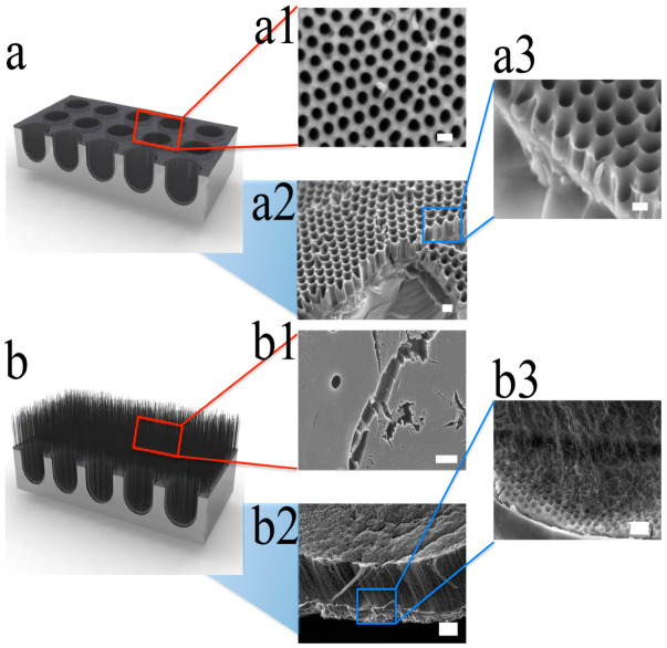
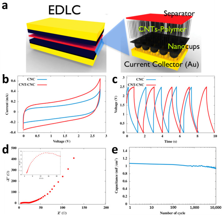
The synthesis of controllable hollow graphitic architectures can engender revolutionary changes in nanotechnology. Here, we present the synthesis, processing, and possible applications of low aspect ratio hollow graphitic nanoscale architectures that can be precisely engineered into morphologies of (1) continuous carbon nanocups, (2) branched carbon nanocups, and (3) carbon nanotubes-carbon nanocups hybrid films. These complex graphitic nanocup-architectures could be fabricated by using a highly designed short anodized alumina oxide nanochannels, followed by a thermal chemical vapor deposition of carbon. The highly porous film of nanocups is mechanically flexible, highly conductive, and optically transparent, making the film attractive for various applications such as multifunctional and high-performance electrodes for energy storage devices, nanoscale containers for nanogram quantities of materials, and nanometrology.

Keywords: carbon nanocup container; flexible and transparent supercapacitor; graphitic nanoscale architecture; precisely controllable nanostructure.


Conflict of interest statement

The authors declare no conflict of interest.

Figures

Figure 1
Figure 1
Schematic of various architectures using the anodized aluminum oxide (AAO) template and their applications: flexible and transparent supercapacitors [37], high-performance supercapacitors [36], and carbon nanocups (CNC) container system [27]. Insert images were reproduced with permission from [27,36,37]. Copyright (2009) American Chemical Society, (2012) American Chemical Society, and (2012) Springer Nature.
Figure 2
Figure 2
SEM and TEM micrographs of a two-dimensional carbon nanocup film structure after removing the AAO template. SEM images show (a) the upside of highly dense carbon nanocup arrays connected with a thin graphite layer, (b) a two-dimensional and flexible film of carbon nanocups, and (c) the side view of carbon nanocups (100 nm diameter and 200 nm length) connected with a graphitic layer of 10 nm thicknesses. Scale bars are 200 nm. (d) A TEM image shows connected arrays of carbon nanocup film with 80 nm diameter and 80 nm length. Scale bar is 50 nm. (e) Raman spectra taken from MWNTs (10 μm in length), long nanocups (180 μm in length), and short nanocups (60 nm in length). Reproduced with permission from [27]. Copyright (2009) American Chemical Society.
Figure 3
Figure 3
SEM images of CNC. SEM images of (a) concave and (b,c) convex, and (df) branched nanocup films. (b) SEM image of convex nanocup film with 80 ± 10 nm in diameter and 140 ± 10 nm in length, and (c) shows a high magnification of (b). (e,f) Cross-sectional views of (d) branched nanocup film, and (f) is a high magnification image of (e), where short carbon nanotubes (25 nm in diameter and 330 ± 10 nm in length) are branched from the bottom of a nanocup. The inset figures, respectively, show schematics of concave, convex, and branched convex nanocup film. Reproduced with permission from [37]. Copyright (2012) Springer Nature.
Figure 4
Figure 4
Schematic drawing of SEM images from CNCs and CNTs−CNC hybrid structure. (a) Schematic illustration of CNC. (a1) SEM image on the top surface of CNC, (a2) a low-magnification SEM of the cross-sectional view, and (a3) high-magnification cross-sectional images. The scale bars are 200, 200, and 120 nm, respectively. The images clearly show hollow structures with low aspect ratio. (b) Schematic of vertically aligned CNTs grown on the surface of CNC. (b1) A top-view SEM image of vertically aligned CNTs, (b2) a side view of low-magnification SEM image, and (b3) high-magnification SEM image of a vertically aligned CNTs−CNC structure. The scale bars are 200, 4, and 400 nm, respectively. Reproduced with permission from [36]. Copyright (2012) American Chemical Society.
Figure 5
Figure 5
(a) Schematics of the fabrication process of a branched CNC-based supercapacitor. (be) Electrochemical properties of branched CNC supercapacitor devices: (b) cyclic voltammetry (CV) measured with 10–500 mVs−1 scan rates. (c) Galvanostatic charge/discharge (CD) results measured at constant current density of 5 μAcm−2. (d) The capacitance changes as a function of temperature (20 to 80 °C). (e) Ragone plot (SG: single-layer graphene [54], RMGO: reduced multilayer graphene oxide [54], HGO: hydrated graphitic oxide [56], LSG-EC: laser-scribed graphene electrochemical capacitor [55]). (f,g) Optical pictures demonstrating optical transparency and mechanical flexibility of a large-scale CNC supercapacitor films. Reproduced with permission from [37]. Copyright (2012) Springer Nature.
Figure 6
Figure 6
(a) Schematic of the supercapacitor consisted of two CNT−CNC hybrid structures on Au current collectors. (b) Cyclic voltammograms of supercapacitor cells having CNC and CNT−CNC electrodes, at a scan rate of 1 mV/s in 1 M LiPF6 electrolyte. (c) Galvanostatic charge−discharge behavior of supercapacitor cells with CNC and CNT−CNC electrodes, at an applied constant current of 10 μA in 1 M LiPF6 electrolyte. (d) Complex-plane impedance spectrum of supercapacitor cell having a CNT−CNC electrode, measured at AC amplitude of 10 mV, in 1 M LiPF6 electrolyte. The inset shows the impedance spectrum of the initial state. (e) Areal capacitance vs. cycle number plot of supercapacitors having CNT−CNC electrodes. Reproduced with permission from [36]. Copyright (2012) American Chemical Society.
Figure 7
Figure 7
(a) Schematic of the overall process in making a closed CNC container system filled with different-sized Pb nanoparticles. (b) Large size Pb nanodroplet at 630 K inside nanocontainer. (c) Two small Pb nanodroplets at 600 K inside nanocontainers. (d) The size of Pb nanodroplet gradually decreases in the open CNC container due to evaporation. Originally, at 640 K, the liquid Pb nanodroplet stopped motion and became spherical. After 0.03 s, this stationary Pb droplet moved towards the edge of the nanocontainer. At 670 and 770 K, the nanodroplet formed a meniscus shape. Eventually, the liquid Pb changed to a hollow, concave shape at 820, 825, 830, 835, and 840 K, respectively. All scale bars are 20 nm. Reproduced with permission from [38]. Copyright (2013) Springer Nature.

References

    1. Bendjemil B., Cleymand F., Pichler T., Knupfer M., Fink J. Carbon Nanostructures in Cancer Diagnosis and Therapy. J. Nanom. Nanos Tech. JNNT-110. 2019;2019:1–18.
    1. Bezzon V.D., Montanheiro T.L., de Menezes B.R., Ribas R.G., Righetti V.A., Rodrigues K.F., Thim G.P. Carbon Nanostructure-based Sensors: A Brief Review on Recent Advances. Adv. Mater. Sci. Eng. 2019;2019:4293073. doi: 10.1155/2019/4293073. - DOI
    1. Chu J.O., Dimitrakopoulos C.D., Grill A., McArdle T.J., Pfeiffer D., Saenger K.L., Wisnieff R.L. Carbon Nanostructure Device Fabrication Utilizing Protect Layers. 9,768,288. U.S. Patent. 2017 Sep 19;
    1. Iglesias D., Bosi S., Melchionna M., Da Ros T., Marchesan S. The glitter of carbon nanostructures in hybrid/composite hydrogels for medicinal use. Curr. Top. Med. Chem. 2016;16:1976–1989. doi: 10.2174/1568026616666160215154807. - DOI - PubMed
    1. Kaur J., Gill G.S., Jeet K. Characterization and Biology of Nanomaterials for Drug Delivery. Elsevier; Amsterdam, The Netherlands: 2019. Applications of carbon nanotubes in drug delivery: A comprehensive review; pp. 113–135.