. 2020 Sep 24;13(19):4259.
doi: 10.3390/ma13194259.

Real-Time Optimization of Anti-Reflective Coatings for CIGS Solar Cells

Affiliations

Real-Time Optimization of Anti-Reflective Coatings for CIGS Solar Cells

Grace Rajan et al. Materials (Basel). .

Abstract

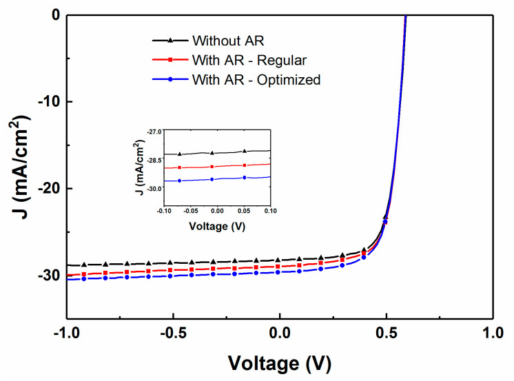
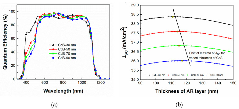
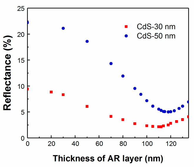
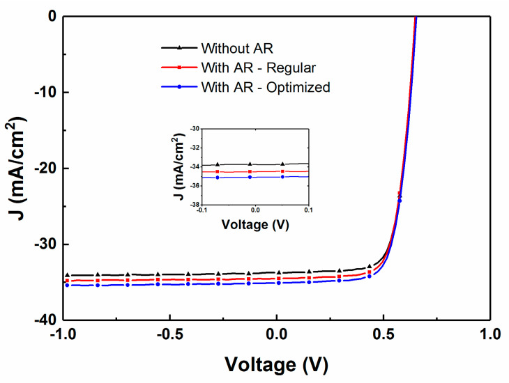
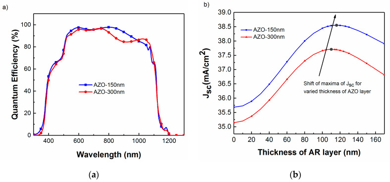
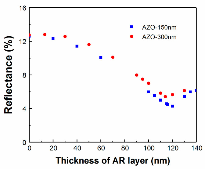
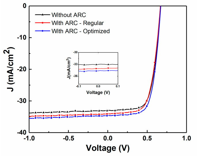
A new method combining in-situ real-time spectroscopic ellipsometry and optical modeling to optimize the thickness of an anti-reflective (AR) coating for Cu(In,Ga)Se2 (CIGS) solar cells is described and applied directly to fabricate devices. The model is based on transfer matrix theory with input from the accurate measurement of complex dielectric function spectra and thickness of each layer in the solar cell by spectroscopic ellipsometry. The AR coating thickness is optimized in real time to optically enhance device performance with varying thickness and properties of the constituent layers. Among the parameters studied, we notably demonstrate how changes in thickness of the CIGS absorber layer, buffer layers, and transparent contact layer of higher performance solar cells affect the optimized AR coating thickness. An increase in the device performance of up to 6% with the optimized AR layer is demonstrated, emphasizing the importance of designing the AR coating based on the properties of the device structure.

Keywords: AR coating; CIGS; ellipsometry; solar cell.


Conflict of interest statement

The authors declare no conflict of interest.

Figures

Figure 1
Figure 1
(a). Experimental ellipsometric spectra in ψ and ∆ along with the best fit for a specific CIGS solar cell device without an anti-reflective (AR) layer along with (b) the layer structure arising from that analysis.
Figure 2
Figure 2
A general multilayer structure having z layers of thickness dm drawn assuming normal incidence.
Figure 3
Figure 3
Simulated external quantum efficiency (QE) and short-circuit current density (JSC) from TMT models for various thickness of the AR layer for the CIGS solar cell characterized by SE (Figure 1).
Figure 4
Figure 4
Comparison of the measured and optically simulated QE spectra for the CIGS solar cell characterized by SE in Figure 1.
Figure 5
Figure 5
(a) Real-time variation of the reflectance during the course of deposition of the AR layer (t = 3 to 12 min). (b) Real-time variation of the reflectance of the CIGS structure with increased thickness of the AR layer.
Figure 6
Figure 6
Comparison of measured (a) current–voltage (J–V) characteristics under simulated 1-sun illuminations and (b) QE spectra obtained for CIGS solar cells with and without the AR coating.
Figure 7
Figure 7
(a) Simulated QE with varied CIGS layer thickness and a fixed 111 nm thick MgF2 layer. (b) Simulated JSC as a function of MgF2 thickness, for varied CIGS layer thickness.
Figure 8
Figure 8
Real-time reflectance for CIGS devices with different CIGS layer thickness.
Figure 9
Figure 9
Measured J–V curves for CIGS solar cells with a 1.5 µm thick absorber and either no AR coating, a 105 nm prior modeled AR coating thickness, or a 95 nm in-situ optimized AR coating thickness.
Figure 10
Figure 10
(a) Simulated QE with varied CdS layer thickness for a fixed 112 nm thick MgF2 layer. (b) Simulated JSC as a function of MgF2 thickness for various CdS thickness.
Figure 11
Figure 11
Real-time reflectance for CIGS devices with different layers of CdS thickness.
Figure 12
Figure 12
Measured J–V curves for CIGS solar cells with a 30 nm thick CdS layer and either no AR coating, a 118 nm prior modeled AR coating thickness, or a 110 nm in-situ optimized AR coating thickness (insert: close up of the −0.1 V to 0.1 V zone).
Figure 13
Figure 13
(a) Simulated QE for varied AZO layer thickness with a fixed 110 nm MgF2 AR layer. (b) Simulated JSC as a function of MgF2 thickness for various AZO layer thickness.
Figure 14
Figure 14
Real-time reflectance for CIGS devices with different AZO layer thickness.
Figure 15
Figure 15
Comparison of the effect of optimized ARC on measured J–V curves for CIGS solar cells with a 150 nm thick AZO layer and either no AR coating, a 105 nm prior modeled AR coating thickness, or a 120 nm in-situ optimized AR coating thickness (insert: close up of the −0.1 V to 0.1 V zone).

References

    1. Jackson P., Wuerz R., Hariskos D., Lotter E., Witte W., Powalla M. Effects of heavy alkali elements in Cu(In,Ga)Se2 solar cells with efficiencies up to 22.6% Phys. Status Solidi RRL Rapid Res. Lett. 2016;10:583–586. doi: 10.1002/pssr.201600199. - DOI
    1. Raut H.K., Ganesh V.A., Nairb A.S., Ramakrishna S. Anti-reflective coatings: A critical, in-depth review. Energy Environ. Sci. 2011;4:3779–3804. doi: 10.1039/c1ee01297e. - DOI
    1. Kaminski P., Lisco F., Walls J. Multilayer broadband antireflective coatings for more efficient thin film CdTe solar cells. IEEE J. Photovolt. 2014;4:452–456. doi: 10.1109/JPHOTOV.2013.2284064. - DOI
    1. Nubile P. Analytical design of antireflection coatings for silicon photovoltaic devices. Thin Solid Films. 1999;342:257–261. doi: 10.1016/S0040-6090(98)01446-1. - DOI
    1. Hara T., Maekawa T., Minoura S., Sago Y., Niki S., Fujiwara H. Quantitative assessment of optical gain and loss in submicron-textured CuInGaSe2 solar cells fabricated by three-stage coevaporation. Phys. Rev. Appl. 2014;2:034012. doi: 10.1103/PhysRevApplied.2.034012. - DOI

LinkOut - more resources