. 2018:187-188:https://doi.org/10.1016/j.mee.2017.11.010.

Optical fiber Fabry-Pérot micro-displacement sensor for MEMS in-plane motion stage

Affiliations

Optical fiber Fabry-Pérot micro-displacement sensor for MEMS in-plane motion stage

Yong-Sik Kim et al. Microelectron Eng. 2018.

Abstract

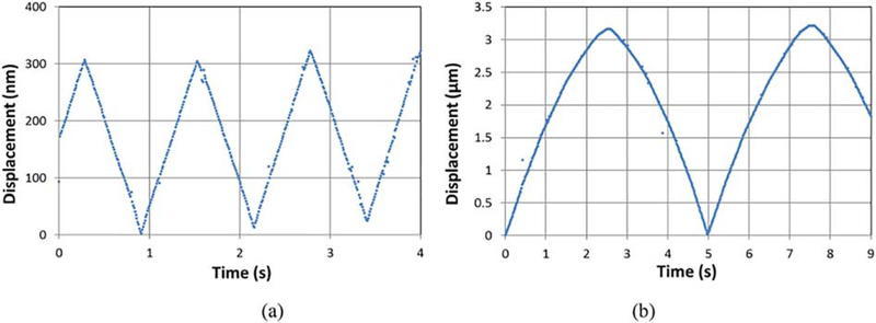
Fabry-Pérot interferometer sensors have been widely used in Micro-Electro-Mechanical-Systems (MEMS) due to high displacement accuracy and immunity to electromagnetic noises, but they are still limited by micro scale measurement range. In this paper, a Fabry-Pérot interferometer in-plane displacement sensor is proposed for measuring the displacement of MEMS devices utilizing a polished optical fiber and a modulated laser source. The polished optical fiber and a sidewall of a MEMS device form an optical cavity for the proposed sensor. The sinusoidal phase modulation with extreme point search algorithm enables the proposed sensor to measure displacements larger than the wavelengths of the laser light in real time. The experimental results show that the proposed displacement sensor has a capability to measure displacements larger than 3 μm and it shows the measurement accuracy less than 35 nm. The proposed displacement sensor is then embedded on a single degree-of-freedom MEMS motion stage and tested to monitor its displacement in real time.

Keywords: Displacement sensor; Distributed feedback laser; Fabry-Pérot interferometry; MEMS; Optical fiber; Phase lock; Sinusoidal phase modulation.


Figures

Fig. 1.
Fig. 1.
A schematic diagram of the proposed FPI displacement sensor [18].
Fig. 2.
Fig. 2.
The relationship between the interferometric signal in blue solid lines and the reference signal Zcos(ωct) of Eq. (3) in black dashed line are plotted for; (a) Z = π/2, (b) Z = 3π/2, (c) Z = 3π/4, (d) Z = π, (e) an interferometric signal changes (shown a red or black points) when the target is in movement, (f) another interferometric signal when the target is in movement. (red dots: global maximum/minimum, black dots: local maximum/minimum).
Fig. 3.
Fig. 3.
The interferometric signal and the reference signal with Z = π: the reference signal Zcos(wt) in Eq. (3) is plotted with a dashed black line and a corresponding interferometric signal in red solid line. Five important interferometric signal values are marked from S0 to S4 and corresponding time stamps indicated from A0 to A4.
Fig. 4.
Fig. 4.
Experimental set-up of the proposed FPI sensor for measurement of a step-height.
Figure 5.
Figure 5.
Comparison of the proposed FPI sensor and the commercial laser interferometer with 0.1 Hz triangular motion of 7 μm stroke.
Fig. 6.
Fig. 6.
The 3D design of the proposed system for MEMS device: (a) overview of the proposed sensor installed on one-DOF MEMS motion stage, (b) the zoomed view of the sidewall of the moving platform circled in (a).
Fig. 7.
Fig. 7.
MEMS fabrication process based on SOI-MUMPs: (a) SOI wafer; (b) metal pad deposition; (c) first etching for the guiding trench; (d) second etching for the guiding trench and third etching for the main components of the MEMS motion stage; (e) fourth etching of the backside of the motion stage; (f) removal of the buried oxide layer to release the motion stage; (g) packaging or installing on a chip; (h) electrical connection and installation of the optical fiber.
Fig. 8.
Fig. 8.
A fabricated MEMS motion stage for the proposed FPI sensor: (a) an overall view (SEM image); (b) the guiding trench near the sidewall of the moving platform (SEM image), (c) the surface roughness of the trench sidewall and the top surface (SEM image), and (d) the embedded optical fiber on the guiding trench (optical image).
Fig. 9.
Fig. 9.
Experimental observations of the motions of a MEMS motion stage: (a) the measured displacements of a 1 Hz triangular motion, and (b) the measured displacements of a 0.2 Hz sinusoidal motion.

References

    1. Heckert NA, “An EDA approach to experimental design.”
    1. Sahu B, Leang KK, Taylor CR, Emerging challenges of microactuators for nanoscale positioning, assembly, and manipulation, J. Manuf. Sci. Eng. 132 (3) (2010) 030917.
    1. Chowdhury S, et al., Automated cell transport in optical tweezers-assisted microfluidic chambers, IEEE Trans. Autom. Sci. Eng. 10 (4) (October 2013) 980–989.
    1. Zamurovic SHYSA, Dagalakis NG, Lee RD, Kim YS, Embedded capacitive displacement sensor for nanopositioning applications, Proceedings of the Conference on Precision Electromagnetic Measurements, 2010.
    1. Chu LL, Gianchandani YB, A micromachined 2D positioner with electrothermal actuation and sub-nanometer capacitive sensing, J. Micromech. Microeng. 13 (2) (2003) 279.

LinkOut - more resources