. 2020 Oct 15;10(10):2039.
doi: 10.3390/nano10102039.

Recent Advances in the Development of Nano-Sculpted Films by Magnetron Sputtering for Energy-Related Applications

Affiliations

Recent Advances in the Development of Nano-Sculpted Films by Magnetron Sputtering for Energy-Related Applications

Adriano Panepinto et al. Nanomaterials (Basel). .

Abstract

In this paper, we overview the recent progress we made in the magnetron sputtering-based developments of nano-sculpted thin films intended for energy-related applications such as energy conversion. This paper summarizes our recent experimental work often supported by simulation and theoretical results. Specifically, the development of a new generation of nano-sculpted photo-anodes based on TiO2 for application in dye-sensitized solar cells is discussed.

Keywords: DSSCs; GLAD; growth simulations; magnetron sputtering; nano-sculpted films.


Conflict of interest statement

The authors declare no conflict of interest.

Figures

Figure 1
Figure 1
Schematic description of the ballistic shadowing effect during thin-film growth in glancing angle geometry (reproduced from [25], Hindawi, 2012).
Figure 2
Figure 2
Sketch of the deposition chamber used in this work (reproduced from [32], MDPI, 2019).
Figure 3
Figure 3
Kinetic Monte Carlo simulation strategy.
Figure 4
Figure 4
Structure zone diagram of Movchan and Demchishin applicable to the film growth by physical vapor deposition (PVD) (reproduced from [48] with permission from Springer, 2014).
Figure 5
Figure 5
SEM (scanning electron microscopy) cross-sectional view with the corresponding simulation of: (a) Ti and (b) Mg columnar films deposited with α = 85°. Evolution of the columnar tilt angle (β) as a function of the angle of deposition (α) for (c) Ti and (d) Mg nano-sculpted thin films. The error bars were estimated by taking the tilt average over 20 columns (adapted from [50] with permission from Elsevier, 2017, and from [32], MDPI, 2019).
Figure 6
Figure 6
Ti thin films synthesized at 150 W and 85° for various deposition pressures: (a) 0.13; (b) 0.26; (c) 0.65; (d) 1.3 Pa with the corresponding simulations. The red angle accounts for the average columnar tilt angle (β) estimated by over 20 columns (adapted from [50] with permission from Elsevier, 2017).
Figure 7
Figure 7
Columnar tilt angle as a function of the deposition pressure for experimental and simulated thin films. The blue line corresponds to the evolution of the mean free path of the sputtered Ti atoms calculated from Equation (1) (reproduced from [50] with permission from Elsevier, 2017).
Figure 8
Figure 8
Ti thin films synthesized at 150 W, 0.13 Pa, and 85° for various substrate temperatures: (a) 373; (b) 523; (c) 723; (d) 873 K with the corresponding simulations. The red angle accounts for the average columnar tilt angle (β) estimated by over 20 columns (adapted from [50] with permission from Elsevier, 2017).
Figure 9
Figure 9
Mg thin films synthesized at 50 W, 0.26 Pa, and 85° for various substrate temperatures: (a) 313; (b) 353; (c) 433; (d) 473; (e) 573 K.
Figure 10
Figure 10
Ti thin films (150 W, 0.13 Pa, 85°) deposited at various rotations of the substrate to generate: (ac) Zigzag structures; (d) helicoidal structures at 0.1°/s; vertical pillars at (e) 1.0°/s and (f) 10.0°/s with the corresponding simulations. The red angle accounts for the average columnar tilt angle (β) (adapted from [50] with permission from Elsevier, 2017).
Figure 11
Figure 11
Evolution of the porosity as a function of the aspect ratio for Mg nano-sculpted films deposited at various deposition pressures and α. The inset illustrates the definition of the aspect ratio, Г (adapted from [32], MDPI, 2019).
Figure 12
Figure 12
Kinetic Monte Carlo (kMC) tri-dimensional (3D) analyses of the effective porosity for different conditions with pore sizes above 0.64 nm (M1) and above 3.2 nm (M2) (reproduced from [50] with permission from Elsevier, 2017).
Figure 13
Figure 13
(a) Transmission electron microscopy (TEM) image of a Ti micro-column constituted by nano-columns from a Ti thin film synthesized at 0.13 Pa, 150 W, and 85°; (b) the corresponding kMC simulation where each atom is represented by its covalent radius (reproduced from [50] with permission from Elsevier, 2017).
Figure 14
Figure 14
Cross-sectional SEM images of nano-columnar (a) TiO2 and (b) Ti thin film deposited at 150 W, 0.13 Pa, and α = 85°. Cross-sectional SEM images of helicoidal (c) TiO2 and (d) Ti thin film deposited at 150 W, 0.13 Pa, α = 85°, and фs = 0.1°/s (adapted from [50] and [9] with permission from Elsevier, 2017 and 2015, respectively).
Figure 15
Figure 15
Cross-sectional SEM images of nano-columnar (a) Mg and (b) MgO thin film deposited at 50 W, 0.26 Pa, and α = 85°. The white angle accounts for the average columnar tilt angle (β) estimated by over 20 columns.
Figure 16
Figure 16
Growth models expected for oblique angle deposition at different substrate temperatures (reproduced from [50] with permission from Elsevier, 2017).
Figure 17
Figure 17
Schematic electron transport pathway in dye-sensitized solar cells (DSSCs).
Figure 18
Figure 18
High-resolution TEM picture of an isolated column from a slanted columnar TiO2 thin film annealed 2 h at 773 K; (a) the corresponding electron diffraction patterns; (b) high-magnification pictures at various locations.
Figure 19
Figure 19
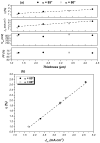
(a) Photovoltaic performances of liquid DSSCs integrating a slanted columns-based TiO2 film as the photo-anode and according to the thickness of the latter; (b) plot of the cell efficiency according to the corresponding Jsc.
Figure 20
Figure 20
Cross-sectional SEM picture of a slanted columnar thin film (4.3 μm) after spin coating by a TiO2 nanoparticles solution.
Figure 21
Figure 21
(a) Photovoltaic performances of DSSCs based on various photo-anode architectures. Schematic representation of the electron transfer occurring in photo-anode based on: (b) Slanted columnar thin film; (c) the combination of slanted columns and nanoparticles; (d) nanoparticulate thin films.

References

    1. Hawkeye M.M., Taschuk M.T., Brett M.J. Glancing Angle Deposition of Thin Films. Wiley; Hoboken, NJ, USA: 2014.
    1. O’Regan B., Grätzel M. A low-cost, high-efficiency solar cell based on dye-sensitized colloidal TiO2 films. Nature. 1991;353:737–740. doi: 10.1038/353737a0. - DOI
    1. Forro L., Chauvet O., Emin D., Zuppiroli L. High mobility n-type charge carriers in large single crystals of anatase (TiO2) J. Appl. Phys. 1994;75:633–635. doi: 10.1063/1.355801. - DOI
    1. Agrell H.G., Boschloo G., Hagfeldt A. Conductivity Studies of Nanostructured TiO2 Films Permeated with Electrolyte. J. Phys. Chem. B. 2004;108:12388–12396. doi: 10.1021/jp037119p. - DOI
    1. Mor G.K., Shankar K., Paulose M., Varghese O.K., Grimes C.A. Use of Highly-Ordered TiO2 Nanotube Arrays in Dye-Sensitized Solar Cells. Nano Lett. 2006;6:215–218. doi: 10.1021/nl052099j. - DOI - PubMed

LinkOut - more resources