. 2020 Oct 30;11(1):5483.
doi: 10.1038/s41467-020-19331-6.

Electron tunneling at the molecularly thin 2D perovskite and graphene van der Waals interface

Affiliations

Electron tunneling at the molecularly thin 2D perovskite and graphene van der Waals interface

Kai Leng et al. Nat Commun. .

Abstract

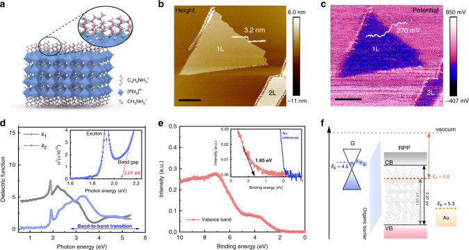
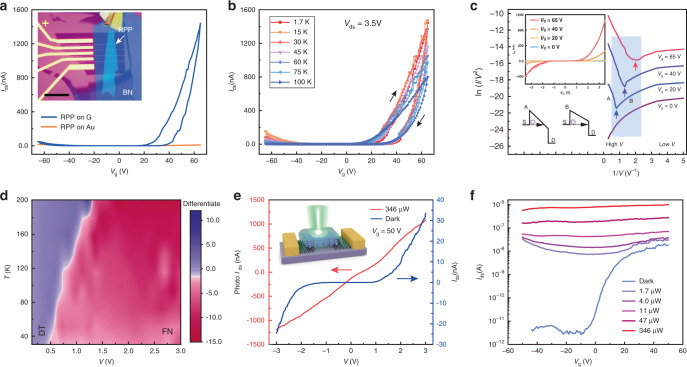
Quasi-two-dimensional perovskites have emerged as a new material platform for optoelectronics on account of its intrinsic stability. A major bottleneck to device performance is the high charge injection barrier caused by organic molecular layers on its basal plane, thus the best performing device currently relies on edge contact. Herein, by leveraging on van der Waals coupling and energy level matching between two-dimensional Ruddlesden-Popper perovskite and graphene, we show that the plane-contacted perovskite and graphene interface presents a lower barrier than gold for charge injection. Electron tunneling across the interface occurs via a gate-tunable, direct tunneling-to-field emission mechanism with increasing bias, and photoinduced charge transfer occurs at femtosecond timescale (~50 fs). Field effect transistors fabricated on molecularly thin Ruddlesden-Popper perovskite using graphene contact exhibit electron mobilities ranging from 0.1 to 0.018 cm2V-1s-1 between 1.7 to 200 K. Scanning tunneling spectroscopy studies reveal layer-dependent tunneling barrier and domain size on few-layered Ruddlesden-Popper perovskite.


Conflict of interest statement

The authors declare no competing interests.

Figures

Fig. 1
Fig. 1. Spectroscopic analysis of Fermi level and band edges in Ruddlesden-Popper perovskite (RPP) relative to graphene (G) and gold (Au).
a Structural illustration of monolayer n = 4 RPP ((C4H9NH3)2(CH3NH3)3Pb4I13). b Atomic force microscopy (AFM) image of monolayer and bilayer n =. 4 RPP flakes exfoliated on pure silicon substrate. Scale bar, 1 µm. c Corresponding Kelvin probe force microscopy (KPFM) on the same area of (b). Scale bar, 1 µm. d Real (Ɛ1) and imaginary (Ɛ2) components of the dielectric function for n = 4 RPP; inset shows the extrapolated electronic gap. e Valence band spectroscopy of n = 4 RPP showing valence band edge. f Interfacial energy alignment diagrams of n = 4 RPP, G and Au.
Fig. 2
Fig. 2. Scanning tunneling microscopy (STM) and spectroscopy (STS) on exfoliated n = 4 RPP flakes of different thicknesses on G and Au substrates.
Empty State (+2.3 V, 10 pA) images of a bilayer RPP on G; b monolayer RPP on G; c thick RPP on G. d Monolayer RPP on Au. e Thick RPP on Au. Scale bars, 4 nm (ae). f STS (dI/dV) of n = 4 RPP flakes of different thicknesses on G and Au substrates.
None
2D perovskite FET devices (n = 4) and their photo-electrical characterizations, using G or Au as electrodes.
Fig. 3 a Transfer characteristics of RPP/G and RPP/Au FET devices at 1.7 K. Inset, Optical image of a typical bilayer thick 2D RPP device using G as electrode. Source-drain channel length is 300 nm. Scale bar, 15 µm. b Temperature-dependent transfer characteristics at 1.7–100 K for RPP/G FET. c Fowler-Nordheim (F-N) plots of 2D RPP/G, with each plot collected at a fixed gate voltage. The minimum voltage highlighted by the arrow is the transition point from direct tunneling (DT) to F-N as voltage increases. Schematic diagrams corresponding to F-N tunneling (point A) and DT (point B). Inset, I(V) curves corresponding to the F-N plot. d Temperature-dependent color map of F-N plots. The white line indicates the transition boundary between DT and F-N tunneling. e Output characteristics in the dark and under laser illumination based on 2D RPP/G FET device at 77 K. f Transfer characteristics in the dark and under different illumination intensities for RPP/G device at 77 K.
Fig. 4
Fig. 4. Femtosecond pump-probe study of dynamic photocarrier injection across RPP/G heterostructure.
ac Differential reflectivity spectra of (a) n = 4 RPP flake, b G, and c RPP/G heterostructure as a function of pump-probe delay time and probe wavelength, when pumping at 25 pJ/μm2 peak energy density. d Cross-section of the data plotted in (b and c) at λ = 820 nm. Solid lines in the graph correspond to fits considering exponential growth (t < 0 fs) and decay (t > 0 fs) functions.

Similar articles

Cited by

References

    1. Grancini G, Nazeeruddin MK. Dimensional tailoring of hybrid perovskites for photovoltaics. Nat. Rev. Mater. 2018;4:4–22. doi: 10.1038/s41578-018-0065-0. - DOI
    1. Smith MD, Crace EJ, Jaffe A, Karunadasa HI. The diversity of layered halide perovskites. Annu. Rev. Mater. Res. 2018;48:111–136. doi: 10.1146/annurev-matsci-070317-124406. - DOI
    1. Stoumpos CC, et al. Ruddlesden–Popper hybrid lead iodide perovskite 2D homologous semiconductors. Chem. Mat. 2016;28:2852–2867. doi: 10.1021/acs.chemmater.6b00847. - DOI
    1. Tsai H, et al. High-efficiency two-dimensional Ruddlesden–Popper perovskite solar cells. Nature. 2016;536:312. - PubMed
    1. Yuan M, et al. Perovskite energy funnels for efficient light-emitting diodes. Nat. Nanotechnol. 2016;11:872. doi: 10.1038/nnano.2016.110. - DOI - PubMed