

Structural and electronic switching of a single crystal 2D metal-organic framework prepared by chemical vapor deposition
- PMID: 33139701
- PMCID: PMC7608636
- DOI: 10.1038/s41467-020-19220-y
Structural and electronic switching of a single crystal 2D metal-organic framework prepared by chemical vapor deposition
Abstract
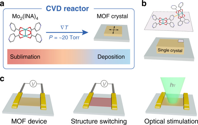
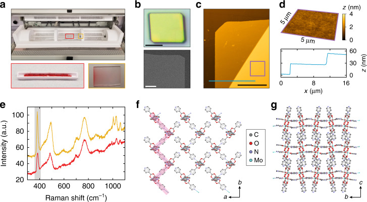
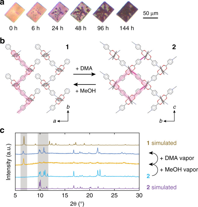
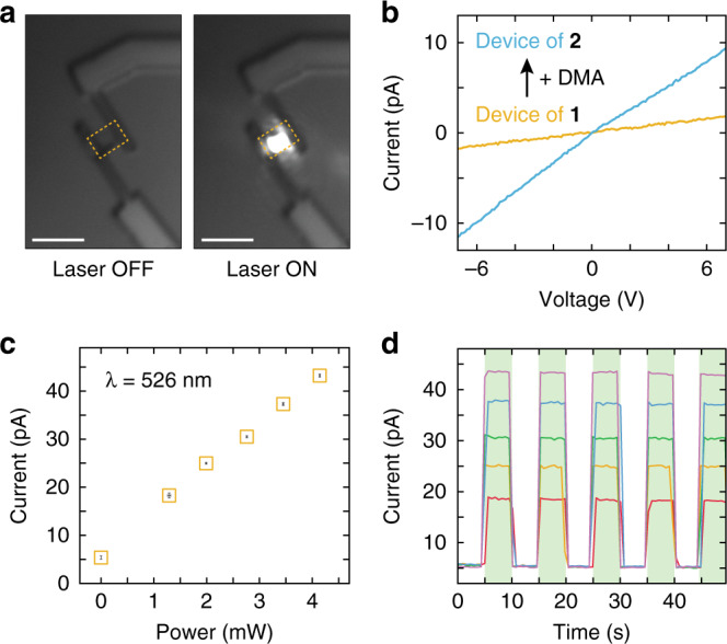
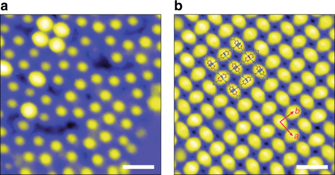
The incorporation of metal-organic frameworks into advanced devices remains a desirable goal, but progress is hindered by difficulties in preparing large crystalline metal-organic framework films with suitable electronic performance. We demonstrate the direct growth of large-area, high quality, and phase pure single metal-organic framework crystals through chemical vapor deposition of a dimolybdenum paddlewheel precursor, Mo2(INA)4. These exceptionally uniform, high quality crystals cover areas up to 8600 µm2 and can be grown down to thicknesses of 30 nm. Moreover, scanning tunneling microscopy indicates that the Mo2(INA)4 clusters assemble into a two-dimensional, single-layer framework. Devices are readily fabricated from single vapor-phase grown crystals and exhibit reversible 8-fold changes in conductivity upon illumination at modest powers. Moreover, we identify vapor-induced single crystal transitions that are reversible and responsible for 30-fold changes in conductivity of the metal-organic framework as monitored by in situ device measurements. Gas-phase methods, including chemical vapor deposition, show broader promise for the preparation of high-quality molecular frameworks, and may enable their integration into devices, including detectors and actuators.
Conflict of interest statement
The authors declare no competing interests.
Figures
Similar articles
-
Bipolar Resistive Switching in 2D MoSe2 Grown by Atmospheric Pressure Chemical Vapor Deposition.ACS Appl Mater Interfaces. 2024 Jan 10;16(1):1767-1778. doi: 10.1021/acsami.3c14215. Epub 2023 Dec 19. ACS Appl Mater Interfaces. 2024. PMID: 38113456
-
Current Progress and Future Directions in Gas-Phase Metal-Organic Framework Thin-Film Growth.ChemSusChem. 2020 Oct 21;13(20):5433-5442. doi: 10.1002/cssc.202001504. Epub 2020 Sep 4. ChemSusChem. 2020. PMID: 32785977
-
Two-dimensional covalent organic framework films prepared on various substrates through vapor induced conversion.Nat Commun. 2022 Mar 17;13(1):1411. doi: 10.1038/s41467-022-29050-9. Nat Commun. 2022. PMID: 35301302 Free PMC article.
-
Recent Developments in Controlled Vapor-Phase Growth of 2D Group 6 Transition Metal Dichalcogenides.Adv Mater. 2019 May;31(20):e1804939. doi: 10.1002/adma.201804939. Epub 2019 Feb 1. Adv Mater. 2019. PMID: 30706541 Review.
-
Low-Temperature Vapor-Phase Growth of 2D Metal Chalcogenides.Small. 2024 May;20(19):e2307587. doi: 10.1002/smll.202307587. Epub 2023 Dec 12. Small. 2024. PMID: 38084456 Review.
Cited by
-
Nanograin network memory with reconfigurable percolation paths for synaptic interactions.Light Sci Appl. 2023 May 15;12(1):118. doi: 10.1038/s41377-023-01168-5. Light Sci Appl. 2023. PMID: 37188669 Free PMC article.
-
Conductive Stimuli-Responsive Coordination Network Linked with Bismuth for Chemiresistive Gas Sensing.ACS Appl Mater Interfaces. 2021 Dec 22;13(50):60306-60318. doi: 10.1021/acsami.1c14453. Epub 2021 Dec 13. ACS Appl Mater Interfaces. 2021. PMID: 34898182 Free PMC article.
-
Manipulation of Valence Trapping through Local Order of Fe3O Units in an Intrinsically Mixed-Valence Coordination Polymer.Inorg Chem. 2025 May 26;64(20):10208-10218. doi: 10.1021/acs.inorgchem.5c01117. Epub 2025 May 15. Inorg Chem. 2025. PMID: 40375572
-
Directing the Morphology, Packing, and Properties of Chiral Metal-Organic Frameworks by Cation Exchange.Angew Chem Int Ed Engl. 2022 Aug 22;61(34):e202205238. doi: 10.1002/anie.202205238. Epub 2022 Jun 28. Angew Chem Int Ed Engl. 2022. PMID: 35594390 Free PMC article.
-
Design Strategies for Enhanced Conductivity in Metal-Organic Frameworks.ACS Cent Sci. 2021 Mar 24;7(3):445-453. doi: 10.1021/acscentsci.1c00047. Epub 2021 Feb 11. ACS Cent Sci. 2021. PMID: 33791427 Free PMC article. Review.
References
-
- Medina DD, Mähringer A, Bein T. Electroactive metalorganic frameworks. Isr. J. Chem. 2018;58:1089–1101. doi: 10.1002/ijch.201800110. - DOI
