. 2020 Nov 6;10(1):19266.
doi: 10.1038/s41598-020-74881-5.

Micro-combinatorial sampling of the optical properties of hydrogenated amorphous [Formula: see text] for the entire range of compositions towards a database for optoelectronics

Affiliations

Micro-combinatorial sampling of the optical properties of hydrogenated amorphous [Formula: see text] for the entire range of compositions towards a database for optoelectronics

Benjamin Kalas et al. Sci Rep. .

Abstract

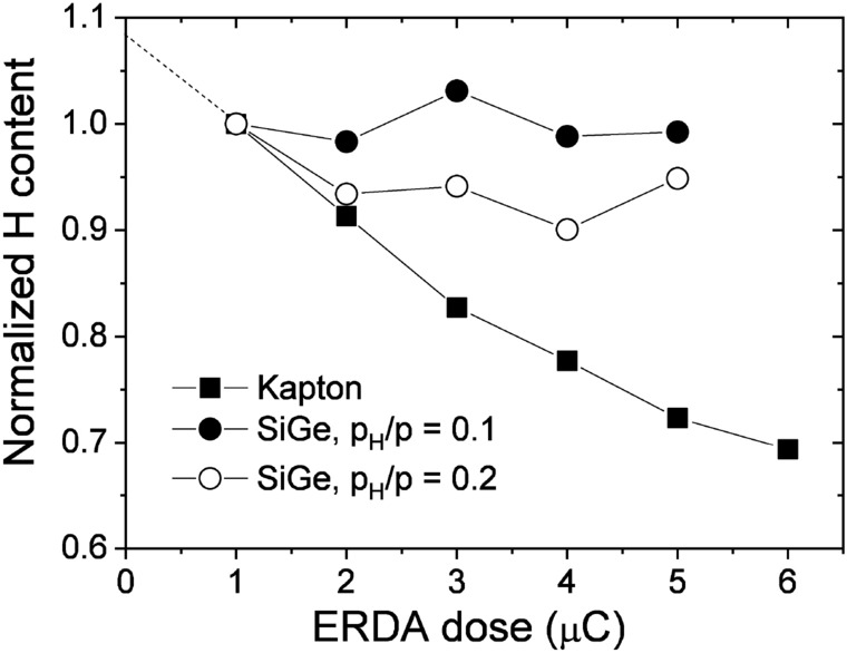
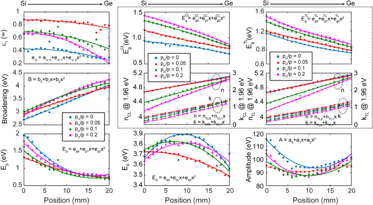
The optical parameters of hydrogenated amorphous a-[Formula: see text]:H layers were measured with focused beam mapping ellipsometry for photon energies from 0.7 to 6.5 eV. The applied single-sample micro-combinatorial technique enables the preparation of a-[Formula: see text]:H with full range composition spread. Linearly variable composition profile was revealed along the 20 mm long gradient part of the sample by Rutherford backscattering spectrometry and elastic recoil detection analysis. The Cody-Lorentz approach was identified as the best method to describe the optical dispersion of the alloy. The effect of incorporated H on the optical absorption is explained by the lowering of the density of localized states in the mobility gap. It is shown that in the low-dispersion near infrared range the refractive index of the a-[Formula: see text] alloy can be comprehended as a linear combination of the optical parameters of the components. The micro-combinatorial sample preparation with mapping ellipsometry is not only suitable for the fabrication of samples with controlled lateral distribution of the concentrations, but also opens new prospects in creating databases of compounds for optical and optoelectonic applications.


Conflict of interest statement

The authors declare no competing interests.

Figures

Figure 1
Figure 1
Setup used for the “single-sample concept” combinatorial deposition of the a-Si1-xGex:H layers.
Figure 2
Figure 2
Normalized H contents as a function of the measurement dose for 1.6 MeV He+ ERDA experiments. Squares represent data for Kapton as reference for H, while full and open dots denote samples ‘C’ and ‘D’ (pH/p=0.1 and 0.2), respectively. The dotted line shows linear extrapolation to zero dose for sample ‘D’.
Figure 3
Figure 3
Left-hand side: atomic fractions of Si and Ge showing the incorporated H for pH/p=0.2 of the SiGe layer along the 20 mm length of the sample measured by RBS. Right-hand side: atomic fractions of H evaluated from ERDA spectra applying spectrum simulations by the RBX software for samples ‘C’ and ‘D’ (pH/p=0.1 and 0.2, respectively). Solid lines show linear fits to the data. Note that the test results of H loss were taken into account in the evaluation of the H content as shown in Fig. 2.
Figure 4
Figure 4
Real and imaginary parts of the complex refractive indices of a-Si1-xGex:H thin films (left and right column, respectively) with different partial pressures of H (pH/p=0,0.05, 0.1 and 0.2) as a function of both the lateral position along the 20 mm long gradient section and photon energy. In accordance with the RBS plots, the zero position corresponds to the Si-rich side of the sample. (A Supplementary Information S1 with all the values plotted here are attached to the article.) (Spectra of pH/p=0.1 is removed at position 8 mm).
Figure 5
Figure 5
Real and imaginary parts of the complex refractive indices of a-Si1-xGex:H with pH/p=0.1 for different compositions (left-hand side) and for different H contents for the Si-rich side given as pH/p values written next to the corresponding curves (right-hand side).
Figure 6
Figure 6
Optical properties of sample ‘C’ calculated by the CL model (dashed black lines) and by numerical inversion (colored lines with filled error bars) for three different locations on the sample. (The error bars for both n and k from the numerical inversion are magnified by a factor of 5 (Top figure) for a better visualization.)
Figure 7
Figure 7
Comparison of the complex refractive index of a-Si (left-hand side) and a-Ge (right-hand side). The data are from Jellison et al., Palik et al., Aspnes et al., Serényi et al., Adachi, Lohner et al.[submitted] and Donovant et al..
Figure 8
Figure 8
Quality of fit (RMSE—the smaller the better—see section “Methods”) along sample ‘D’ (pH/p=0.2). The RMSE values related to the CL and TL models are shown using blue and red dotted lines, respectively. For both models, the best fit was achieved by using a graded layer, resulting in low values of inhomogeneity inside the a-Si1-xGex layer. On the right-hand side, the percentage of the inhomogeneity is presented for both models.
Figure 9
Figure 9
Optical gaps of a-Si1-xGex samples and the real and imaginary parts of the complex refractive indices at the wavelength of 633 nm (photon energy of 1.96 eV) modeled by CL (left-hand side) and TL (right-hand side) oscillators (graphs in the dotted frame). The other graphs show the x dependence of the fitted parameters utilizing the CL dispersion of Eq. (3), with the Broadening and Amplitude denoted by Γ and A, respectively.
Figure 10
Figure 10
Vegard plots in the linear range of n for all the samples of different pH/p values.
Figure 11
Figure 11
Dispersion of the linearity (R2—defined in Eq. 5) of the complex refractive index (both n and k spectra) with the concentration. The curves of different colors on the top graph correspond to different pH/p values. The highlighted photon energies are the following: A=1.01 eV, B=1.96 eV, C=3.14 eV and D=5.56 eV. The grey areas show the photon energy range of linear behavior of the real and imaginary parts of the complex refractive index for each sample.
Figure 12
Figure 12
Ellipsometry spectra of the non-hydrogenated a-Si1-xGex sample (‘A’) at the Si-rich and Ge-rich sides for different angles of incidence measured (symbols) and fitted (solid lines) by the CL dispersion. The difference between the measured (Ψm,Δm) and calculated (Ψc,Δc) ellipsometric angles is also included (a). The optical model and the schematic measurement configuration are shown on the right-hand side (b).
Figure 13
Figure 13
1.6 MeV He+ (a) RBS and (b) ERDA spectra as a function of the lateral position along the sample, for an a-Si1-xGex:H layer with nominally 20% H content and with deposition rate of 0.4 nm/s. In (a), for comparison, a reference spectrum for a bare Si sample is also shown. Surface edges for Si, Ge, and H are represented by arrows.
Figure 14
Figure 14
Line profiles and AFM topography images on the samples with pH/p=0.05, 0.1 and 0.2.

References

    1. Coucheron DA, et al. Laser recrystallization and inscription of compositional microstructures in crystalline SiGe-core fibres. Nat. Commun. 2016;7:13265. doi: 10.1038/ncomms13265. - DOI - PMC - PubMed
    1. Božanić M, Sinha S. Emerging transistor technologies capable of terahertz amplification: A way to re-engineer terahertz radar sensors. Sensors (Basel, Switzerland) 2019;19:2454. doi: 10.3390/s19112454. - DOI - PMC - PubMed
    1. Guha S, Yang J, Banerjee A. Amorphous silicon alloy photovoltaic research-present and future. Prog. Photovolt. Res. Appl. 2000;8:141–150. doi: 10.1002/(SICI)1099-159X(200001/02)8:1<141::AID-PIP305>3.0.CO;2-I. - DOI
    1. Gribelyuk MA, Fu B, Zhao WW. Measurement of SiGe composition in 3-D semiconductor fin field effect transistor devices. J. Appl. Phys. 2019;125:165306. doi: 10.1063/1.5083952. - DOI
    1. Haller EE. Germanium: From its discovery to SiGe devices. Mater. Sci. Semicond. Process. 2006;9:408–422. doi: 10.1016/j.mssp.2006.08.063. - DOI