. 2020 Nov 5;13(21):4974.
doi: 10.3390/ma13214974.

Geometry Control of Source/Drain Electrodes in Organic Field-Effect Transistors by Electrohydrodynamic Inkjet Printing

Affiliations

Geometry Control of Source/Drain Electrodes in Organic Field-Effect Transistors by Electrohydrodynamic Inkjet Printing

Piotr Sleczkowski et al. Materials (Basel). .

Abstract

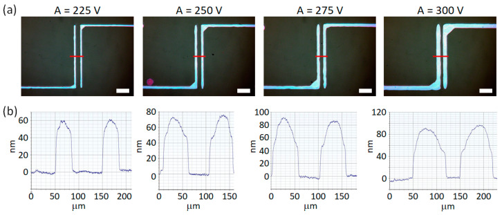
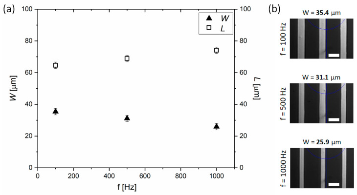
In this work we study the influence of dielectric surface and process parameters on the geometry and electrical properties of silver electrodes obtained by electrohydrodynamic inkjet printing. The cross-section and thickness of printed silver tracks are optimized to achieve a high conductivity. Silver overprints with cross-section larger than 4 μm2 and thickness larger than 90 nm exhibit the lowest resistivity. To fabricate electrodes in the desired geometry, a sufficient volume of ink is distributed on the surface by applying appropriate voltage amplitude. Single and multilayer overprints are incorporated as bottom contacts in bottom gate organic field-effect transistors (OFETs) with a semiconducting polymer as active layer. The multilayer electrodes result in significantly higher electrical parameters than single layer contacts, confirming the importance of a careful design of the printed tracks for reliable device performance. The results provide important design guidelines for precise fabrication of electrodes in electronic devices by electrohydrodynamic inkjet printing.

Keywords: electrohydrodynamic inkjet printing; organic field-effect transistors; printed electronics.


Conflict of interest statement

The authors declare no conflict of interest.

Figures

Figure 1
Figure 1
(a) Schematic top view representation of DGP overprints with various interline spacing (s) and different number of printing passes (n). (b) Exemplary cross-section profile underlining the geometrical parameters W, L and hmax.
Figure 2
Figure 2
Optical microscope images of DGP overprints on SiO2 surface with different types of treatment. Scale bar equal 100 μm.
Figure 3
Figure 3
(a) Optical microscope images of DGP printed lines on plasma-treated SiO2 surface with different amplitudes (A). (b) Cross-section profiles of the respective overprints. B = 200 V, f = 500 Hz, s = 100 μm. Scale bar equal 200 μm.
Figure 4
Figure 4
Influence of the amplitude of the applied voltage (A) on the geometrical features of the overprints on (a) width (W) and edge-to-edge distance, defining the channel length (L), and (b) maximum height of the overprints (hmax). B = 200 V, f = 500 Hz, s = 100 μm.
Figure 5
Figure 5
(a) Influence of the frequency of the voltage waveform (f) on the linewidth (W) of the overprints and on the resulting channel length (L), for s = 100 μm. (b) Optical microscope images for f = 100 Hz, f = 500 Hz and f = 1000 Hz, respectively. A = 300 V, B = 200 V, s = 100 μm. Scale bar equal 50 μm.
Figure 6
Figure 6
Summary of the geometrical features of the overprints fabricated with different A and f. (a) Width, (b) maximum height and (c) cross-section of the overprints increases for the higher voltage amplitude.
Figure 7
Figure 7
Summary of the resistivity measurements for DGP printed single layer overprints as a function of their cross-section (a) and their maximum height (b) for different A. The blue dashed lines represent the resistivity reported by the ink supplier.
Figure 8
Figure 8
(a) Optical microscope images of DGP overprints on plasma-treated SiO2 surface with different number of printed layers (n). (b) Cross-section profiles of the respective overprints. A = 250 V, B = 200 V, f = 100 Hz, s = 100 µm. Scale bar equal 200 µm.
Figure 9
Figure 9
Summary of the resistivity measurements of single and multilayer overprints. (a) Two-point probe resistivity as a function of the overprint cross-section for different A. (b) Resistivity presented as a function of number of printed layers (n). The blue dashed lines represent the resistivity reported by the ink supplier. B = 200 V, f = 100 Hz.
Figure 10
Figure 10
(a) Transfer and (b) output characteristics of bottom contact/bottom gate organic field-effect transistors (OFETs) with DPP-DTT (poly[2,5-(2-octyldodecyl)-3,6-diketopyrrolopyrrole -alt-5,5-(2,5-di(thien-2-yl)thieno[3,2-b]thiophene)]) as active layer, comprising single (n = 1), double (n = 2) and triple (n = 3) overprints as electrodes. VSD = −40 V for transfer characteristics.

References

    1. Suh Y.H., Shin D.W., Chun Y.T. Micro-to-nanometer patterning of solution-based materials for electronics and optoelectronics. RSC Adv. 2019;9:38085–38104. doi: 10.1039/C9RA07514C. - DOI - PMC - PubMed
    1. Birkholz M., Mai A., Wenger C., Meliani C., Scholz R. Technology modules from micro- and nano-electronics for the life sciences. Wiley Interdiscip. Rev. Nanomed. Nanobiotechnol. 2016;8:355–377. doi: 10.1002/wnan.1367. - DOI - PubMed
    1. Zhang L., Tang Y., Tong L. Micro-/nanofiber optics: Merging photonics and material science on nanoscale for advanced sensing technology. iScience. 2020;23:100810. doi: 10.1016/j.isci.2019.100810. - DOI - PMC - PubMed
    1. Rodriguez S. Redefining microfabrication of high-precision optics: How two-photon grayscale lithography improves quality and throughput of printing microparts. PhotonicsViews. 2020;17:36–39. doi: 10.1002/phvs.202000003. - DOI
    1. Alvarez M.M., Aizenberg J., Analoui M., Andrews A.M., Bisker G., Boyden E.S., Kamm R.D., Karp J.M., Mooney D.J., Oklu R., et al. Emerging trends in micro- and nanoscale technologies in medicine: From basic discoveries to translation. ACS Nano. 2017;11:5195–5214. doi: 10.1021/acsnano.7b01493. - DOI - PubMed

LinkOut - more resources